Electro-active device having metal-containing layer

Inactive Publication Date: 2005-04-21
GENERAL ELECTRIC CO
View PDF18 Cites 18 Cited by
  • Summary
  • Abstract
  • Description
  • Claims
  • Application Information

AI Technical Summary

Benefits of technology

[0007] Accordingly, one aspect of the invention is to provide an electro-active device. The electro-active device comprises: a substrate; a first electrode disposed on a surface of the substrate; a second electrode; at least one electro-active layer disposed between the first electrode and the second electrode, wherein the at least one active layer comprises one of a light absorbing layer and a light emitting layer; and a first metal-containing layer disposed between the electro-active layer and one of the first electrode and the second electrode. The first metal-containing layer comprises at least one metal disposed in a plurality of domains, and at least one of the first electrode and second electrode is a transparent electrode, wherein the first metal-containing layer is adjacent to the transparent layer.

Problems solved by technology

One problem associated with the formation of such metal layers is that they must be deposited using techniques that must be carried out at temperatures at which substrate materials, such as polymeric materials, decompose.
In addition, such vapor deposition-based techniques are frequently carried out under reduced pressure conditions and do not lend themselves to efficient or large-scale manufacture of such electro-active devices.
Metal films have also been deposited by solution-based methods on a substrate at temperatures of about 400° C. However, even this temperature regime is outside the temperature tolerance for many electronic materials and substrates.

Method used


Image

  • Electro-active device having metal-containing layer
  • Electro-active device having metal-containing layer
  • Electro-active device having metal-containing layer

Examples


example 1

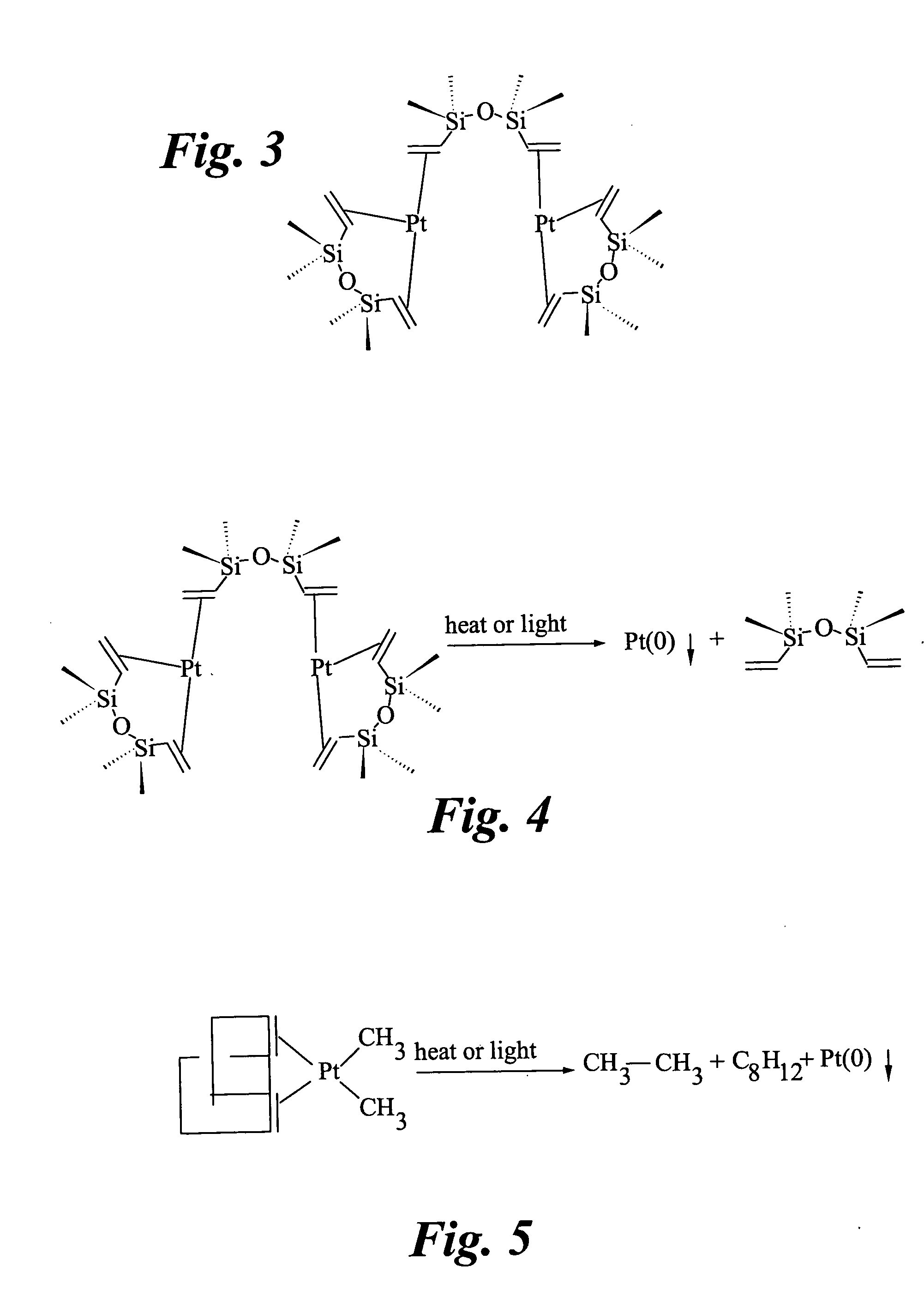
[0045] The initial experiments for low temperature deposition of elemental platinum (Pt(0)) used Karstedt's catalyst solutions. The deposition of elemental platinum using Karstedt's catalyst proceeds according to the reaction shown in FIG. 4. The decomposition temperature was greater than 100° C., and in most instances was about 150° C. Xylene solutions of Karstedt's catalyst were spin coated onto a substrate and then heated to about 150° C. It was later found that better adhesion was obtained when HMDZ (hexamethyldisilazane) was used as a diluent. Cyclic voltammetry (CV) analyses of the Karstedt's catalyst-derived films were consistent with the presence of elemental Pt(0) on the surface of the substrate.

[0046] In some instances, films made using Karstedt's catalyst, produced films that were clear but brown in color. Other Pt precursors having volatile ligands were used to obtain ‘clean’—i.e., substantially residue-free—decomposition to Pt. The precursor dimethyl(1,5-cyclooctadiene...

example 2

[0047] The possible performance of a Pt-containing layer of the present invention in an electro-active device such as a photovoltaic (PV) cell may be correlated with Kelvin probe measurements. The Kelvin probe gives a CPD (contact potential difference) value, which is directly related to the work function of a sample. Thus, a change in CPD value between samples is directly related to a corresponding change in work function; if a standard is known, then the absolute work function of an unknown sample can be determined.

[0048] Platinum-containing layers of the present invention were deposited on two combinations of electrode materials and substrates: tin oxide (SnO) deposited on glass; and indium tin oxide (ITO) deposited on Lexan® (polycarbonate). The CPD values obtained for SnO deposited on glass and ITO on Lexan® were −0.385 V and −0.503 V, respectively.

[0049] The structures of the Pt organometallic complexes that were used to deposit Pt on the electrode / substrate combinations are...


PUM

PropertyMeasurementUnit
Temperatureaaaaaaaaaa

Abstract

An electro-active device, such as a photovoltaic cell or an OLED, is disclosed. The electro-active device comprises a substrate; a first electrode disposed on a surface of the substrate; a second electrode; at least one electro-active layer disposed between the first electrode and the second electrode, wherein the at least one active layer comprises one of a light absorbing layer and a light emitting layer; and a first metal-containing layer disposed between the first electrode and the electro-active layer; and a second metal-containing layer disposed between the least one active layer and one of the first electrode and the second electrode. The first metal-containing layer comprises at least one metal disposed in a plurality of domains. At least one of the first electrode and the second electrode is a transparent electrode. A metal-containing layer for an electro-active device and a method of making such a metal-containing layer are also disclosed.

Description

BACKGROUND OF INVENTION [0001] The invention relates to an electro-active device, such as a photovoltaic cell or an organic light emitting device (OLED). More particularly, the invention relates to a method of depositing a layer of metal at low temperatures to form a metal-containing layer for such an electro-active device. [0002] Certain materials and devices display electronic characteristics, features and uses. Electro-active devices such as photovoltaic cells and organic light emitting diodes (referred hereinafter to as “OLEDs”) are widely used in information displays, solar cells, fuel cell components, and in specialty electronics. One of the features of such devices is a metal-containing conductive or catalytic layer that connects an active light-absorbing or light-emitting material to an electrode, which in turn is deposited on a substrate. [0003] One problem associated with the formation of such metal layers is that they must be deposited using techniques that must be carrie...

Claims


Application Information

Patent Timeline
IPC IPC(8): B05D3/00B05D5/12C23C18/08C23C18/14H01L29/40H05B33/10H01L31/00H01L31/02H01L31/0224H01L31/04H01L33/00H01L51/00H01L51/42H01L51/50H01M14/00H05B33/14H05B33/22H05B33/26
CPCC23C18/08C23C18/14H01L51/0021H01L51/0084H01L51/42Y10T428/26H01L51/5088H01L51/5092Y02E10/542Y02E10/549Y10T428/24917H01L51/441C23C18/143H10K71/60H10K85/341H10K30/00H10K30/81H10K50/171H10K50/17H05B33/26H05B33/10
Inventor LEWIS, LARRY NEILLIU, JIEJANORA, KEVIN HENRY
Owner GENERAL ELECTRIC CO
Why Eureka
Try Eureka