Semiconductor integrated circuit device and semiconductor memory using the same

a technology of integrated circuits and semiconductors, applied in the direction of semiconductor devices, electrical devices, transistors, etc., can solve the problems of ineffective i-type gates, etc., and achieve the effect of enhancing the degree of integration

Inactive Publication Date: 2005-04-21
SEIKO EPSON CORP
View PDF5 Cites 10 Cited by
  • Summary
  • Abstract
  • Description
  • Claims
  • Application Information

AI Technical Summary

Benefits of technology

[0014] At this point, when using the SOI substrate, it is proper for drains of the p-channel and the n-channel transistor to be bonded to each other without going through the element separation area. Since there is no well at a lower part of the drain, there will be no problem with the electrical property. Further, an area of formation of the p-channel and the n-channel transistor may be made small, thus enhancing the degree of integration.
[0015] In an area including a bonded area in which each drain of the p-channel and the n-channel transistor is bonded to each other, impurities injected to the drain area of the p-channel transistor and impurities injected to the drain area of the n-channel transistor may be mixed. When injecting from a slant direction, it is handled by retreating a mask position without widening a distance between gates. When this mask is also used when injecting impurities from a vertical direction, there will be a mixture of two kinds of impurities in the vicinity of the bonded area. Even then, there is no problem with the electrical property, while the distance between the gates may be narrowed, so that the degree of integration is enhanced.

Problems solved by technology

However, the I type gate is not effective particularly when securing a body in contact on the SOI substrate.

Method used


Image

  • Semiconductor integrated circuit device and semiconductor memory using the same
  • Semiconductor integrated circuit device and semiconductor memory using the same
  • Semiconductor integrated circuit device and semiconductor memory using the same

Examples


Embodiment Construction

[0028] Exemplary embodiments according to this invention will be described below with reference to drawings.

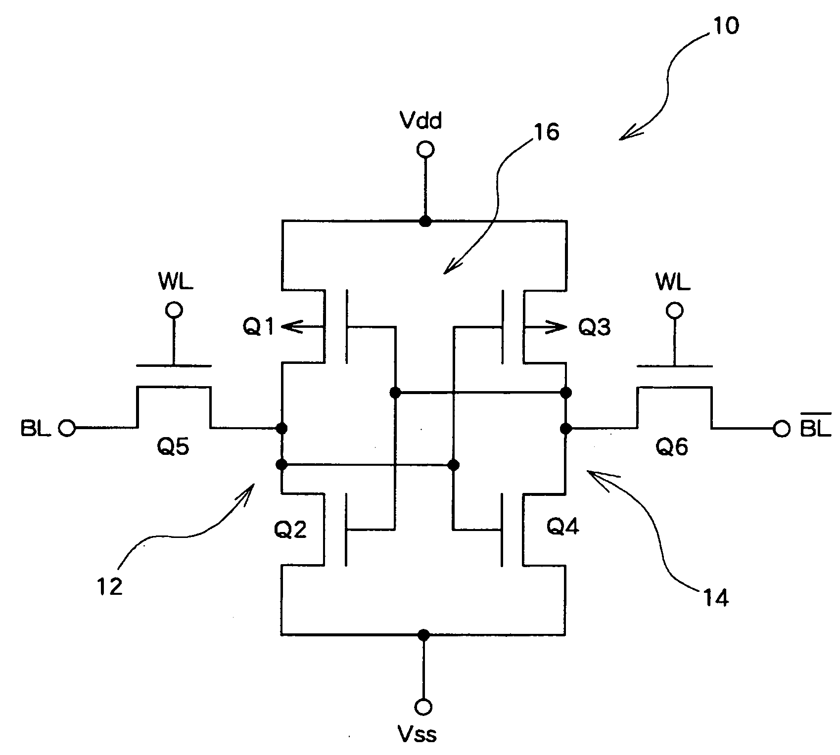
[0029]FIG. 1 is an exemplary circuit diagram of a memory cell of an SRAM which is a semiconductor device of this invention. A memory cell 10 is formed by six MOS electric field effect transistors. A first CMOS inverter 12 is formed by a p-channel load transistor Q1 and a n-channel drive transistor Q2 serially connected thereto. A second CMOS inverter 14 is formed by another p-channel load transistor Q3 and another n-channel drive transistor Q4 serially connected thereto. To a source of the two n-channel drive transistors Q2 and Q4, there is connected a Vss power supply line, while, to a source of the two n-channel drive transistors Q1 and Q3, there is connected a Vdd power supply line. And by cross coupling the first and the second inverter 12 and 14, a flip-flop 16 is formed. This flip-flop 16 is connected to a bit line BL and an inverse bit line {overscore (BL)} by two n-ch...


PUM


Abstract

Aspects of the invention can provide a semiconductor device including a transistor having a gate shape, which enables a source area and a body contact area to be connected without using wiring and with no gate part protruding to the source area side, and a semiconductor memory. The semiconductor device can have field regions, a transistor which includes a gate (L type gate), a gate insulating film directly below the gate, a body area directly below the gate insulating film, and a source area and a drain area formed on both sides which hold the body area in between. The gate can consist essentially of a first part extending along a channel width direction on the field region and a second part protruding from one end of the first part in the channel width direction to the drain side, and being formed in the L type gate in a plan view. A body contact area can be provided on the field region on the opposite side to the first part with the second part of the L type gate in between, and a low resistant layer is formed on a surface between the source area and the body contact area.

Description

BACKGROUND OF THE INVENTION [0001] 1. Field of Invention [0002] Aspects of the invention can relate to a semiconductor device that can have a transistor structure and an inverter structure formed on an SOI (silicon on Insulator) substrate and a semiconductor memory using the same. [0003] 2. Description of Related Art [0004] As a shape of a gate on a field region of a transistor, in addition to a typically used I type gate for a bulk substrate, a T type gate can be used for securing a body contact on the SOI substrate. The I type gate has advantages of a small gate capacity and a minimum of a cell area. However, the I type gate is not effective particularly when securing a body in contact on the SOI substrate. In this respect, the T type gate can be effective for separating a source / drain area from a body contact area, even when a silicide layer is made a surface of the field region on the SOI substrate. However, wiring is required for putting the source area and the body on the same...

Claims


Application Information

Patent Timeline
Patent Type & Authority Applications(United States)
IPC IPC(8): H01L21/8238H01L21/28H01L21/8244H01L21/84H01L27/092H01L27/11H01L27/12H01L29/423H01L29/49H01L29/786
CPCH01L21/84H01L27/1104H01L29/78621H01L29/42384H01L29/78615H01L27/1203H10B10/12
Inventor TAGUCHI, KAZUO
Owner SEIKO EPSON CORP
Why Eureka
Try Eureka