Logic device having vertically extending metal-insulator-metal capacitor between interconnect layers and method of fabricating the same

a technology of metal-insulator metal and logic device, which is applied in the direction of capacitors, semiconductor devices, semiconductor/solid-state device details, etc., can solve the problems of contaminating the dielectric layer, damaging the dielectric layer of the capacitor, and often generating leakage current, so as to improve the leakage current characteristics.

Active Publication Date: 2005-04-28
SAMSUNG ELECTRONICS CO LTD
View PDF18 Cites 77 Cited by
  • Summary
  • Abstract
  • Description
  • Claims
  • Application Information

AI Technical Summary

Benefits of technology

[0015] Exemplary embodiments of the present invention provide a logic device having an MIM capacitor betw...

Problems solved by technology

Because the brim of the lower metal plate is caught by an electric field more than other locations, a leakage current is often generated, unless the thickness of the capacitor dielectric layer is high.
Since the photoresist layer includ...

Method used


Image

  • Logic device having vertically extending metal-insulator-metal capacitor between interconnect layers and method of fabricating the same
  • Logic device having vertically extending metal-insulator-metal capacitor between interconnect layers and method of fabricating the same
  • Logic device having vertically extending metal-insulator-metal capacitor between interconnect layers and method of fabricating the same

Examples


Embodiment Construction

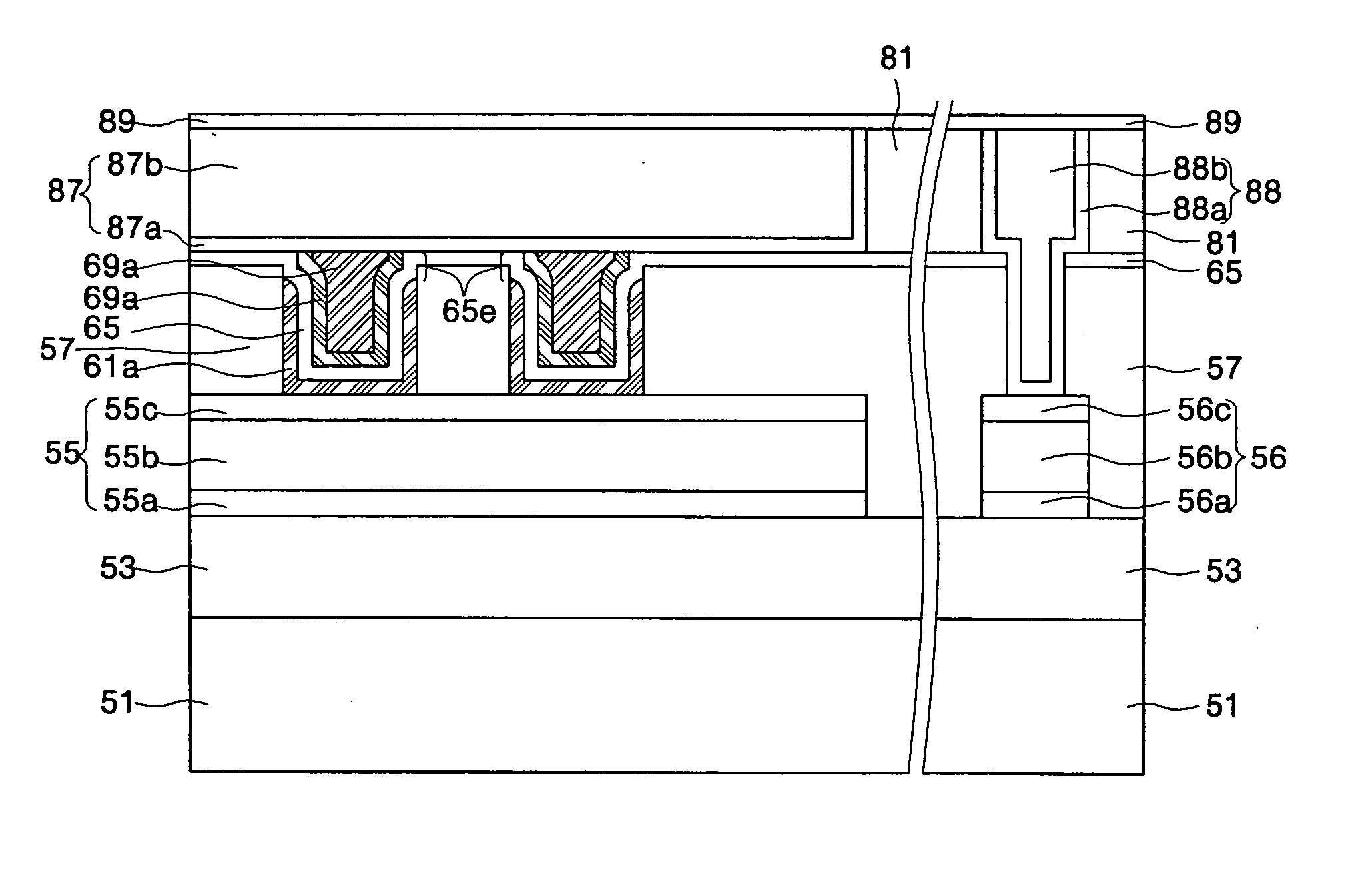
[0033]FIG. 13 is a schematic sectional view illustrating a logic device according to an embodiment of the present invention.

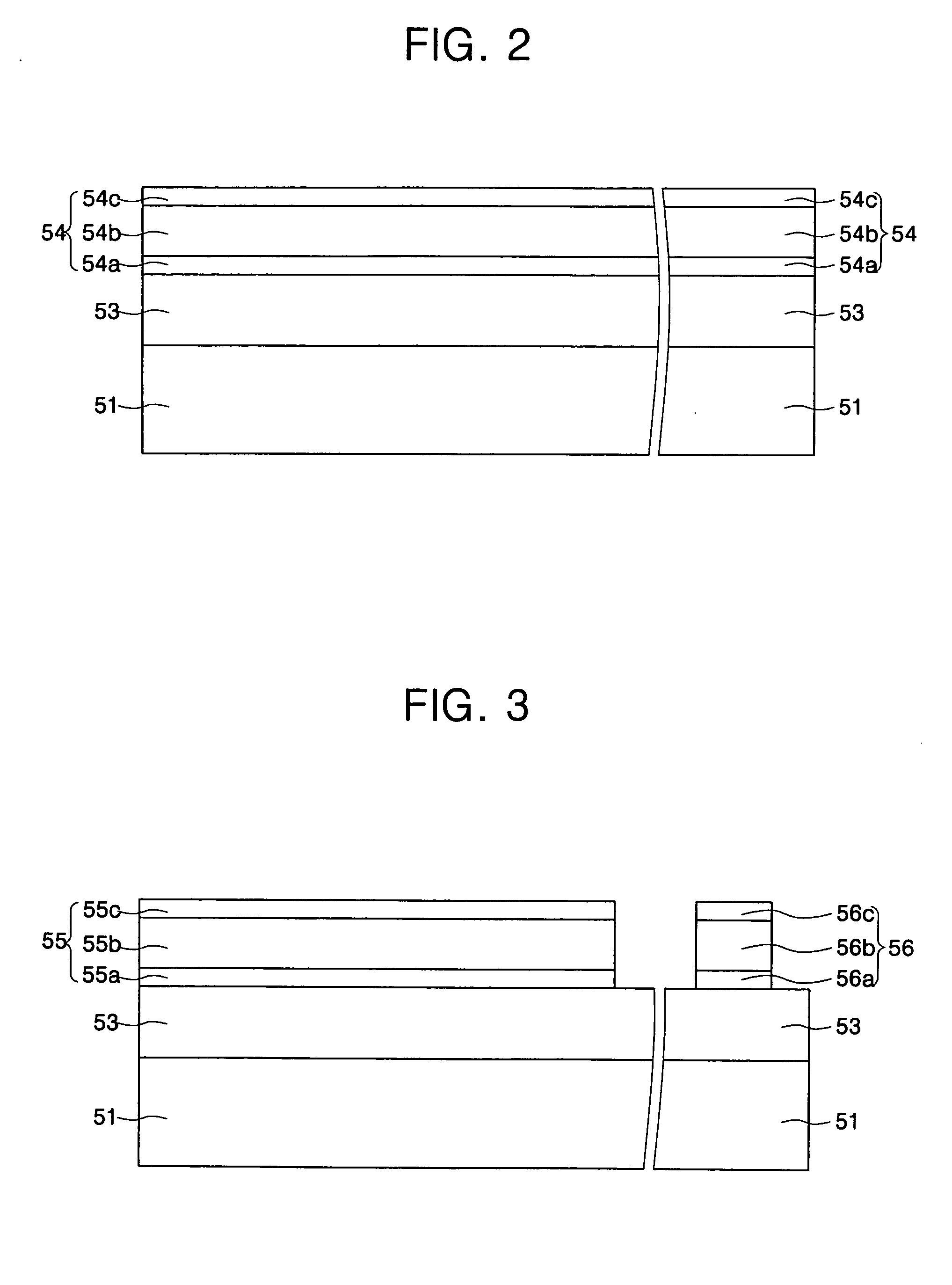
[0034] Referring to FIG. 13, a lower interconnect layer 55 is placed over a semiconductor substrate 51. The lower interconnect layer 55 is separated from the semiconductor substrate 51 by a lower insulating layer 53.

[0035] The lower interconnect layer 55 may be a layered stack including a diffusion barrier layer 55a, a main conductive layer 55b, and a capping layer 55c. The main conductive layer 55b may be formed of aluminum (Al) or copper (Cu), or may be a layered stack of both. Each of the diffusion barrier layer 55a and the capping layer 55c may be titanium (Ti), titanium nitride (TiN), tantalum (Ta), tantalum nitride (TaN), ruthenium (Ru), or tungsten nitride (WN) layer, or may be an at least two-layered stack of those layers.

[0036] An upper interconnect layer 77 is placed over the lower interconnect layer 55. The upper interconnect layer 77 may be a lay...


PUM


Abstract

A logic device having a vertically extending MIM capacitor between interconnect layers includes a semiconductor substrate. A lower interconnect layer is located over the semiconductor substrate, and an upper interconnect layer is located over the lower interconnect layer. A U-shaped lower metal plate is interposed between the lower interconnect layer and the upper interconnect layer. The U-shaped lower metal plate directly contacts the lower interconnect layer. The capacitor dielectric layer covers the inner surface of the lower metal plate. Further, the capacitor dielectric layer has an extension portion interposed between the brim of the lower metal plate and the upper interconnect layer. An upper metal plate covers the inner surface of the capacitor dielectric layer. The upper metal plate is in contact with the upper interconnect layer and is confined by the capacitor dielectric layer.

Description

CROSS-REFERENCE TO RELATED APPLICATION [0001] This application claims priority from Korean Patent Application No. 2003-75650, filed on Oct. 28, 2003, the contents of which are hereby incorporated herein by reference in their entirety as if set forth fully herein. BACKGROUND OF THE INVENTION [0002] 1. Field of the Invention [0003] This disclosure relates to a logic device and a method of fabricating the same and more particularly, to a logic device having a vertically extending metal-insulator-metal capacitor between interconnect layers and a method of fabricating the same. [0004] 2. Description of the Related Art [0005] Generally, a capacitor of a logic device is used as an impedance element. The capacitor used as an impedance element must be linear in its response characteristics. Therefore, a metal-insulator-metal (MIM) capacitor is normally used in the logic device instead of a poly-insulator-poly (PIP) capacitor which exhibits non-linear response characteristics due to charge de...

Claims


Application Information

Patent Timeline
IPC IPC(8): H01L27/10H01L21/02H01L21/768H01L23/48H01L27/08
CPCH01L21/76807H01L28/91H01L27/0805H01L21/76838H01L27/10
Inventor WON, SEOK-JUNJEONG, YONG-KUKKWON, DAE-JINSONG, MIN-WOOKIM, WEON-HONG
Owner SAMSUNG ELECTRONICS CO LTD
Why Eureka
Try Eureka