3C-sic nanowhisker and synthesizing method and 3c-sic nanowhisker

a nanowhisker and nanotechnology, applied in the field of 3c — sic nanowhiskers and synthesizing methods, can solve the problems of not being used in light-emitting devices or light-receiving devices, high cost, and difficult to make devices from this sic whisker, and achieve the effect of convenient handling

Inactive Publication Date: 2005-04-28
JAPAN SCI & TECH CORP +1
View PDF5 Cites 6 Cited by
  • Summary
  • Abstract
  • Description
  • Claims
  • Application Information

AI Technical Summary

Benefits of technology

[0013] According to the method mentioned above, the 3C—SiC nanowhisker which has its root buried in the Si substrate can grow on the substrate surface. Also, by controlling the thickness of said thin film of the metal element, it is possible to grow 3C—SiC single crystal nanowhisker having a desired diameter being proportional to the thickness of said thin film, Further, it is possible to control the length of the 3C—SiC single crystal nanowhisker by controlling said Si substrate temperature.
[0014] According to the synthesizing method of 3C—SiC nanowbisker of the present invention, since it uses solid Si for the source of Si element, it is possible to synthesize 3C—SiC single crystal nanowhisker quite safely and at low cost.
[0020] The 3C—SiC nanowhisker of the present invention can emit visible light owing to quantum confinement effect, and can vary wavelength of the emitted light by the diameter thereof. Therefore, for example, a display device which can emit more than one wavelength can be obtained by forming the 3C—SIC nanowhiskers with various diameters. Also, various electronic devices of making from Si and of light-emitting devices making from 3C—SiC nanowhiskers can be formed on the same Si substrate. Since the nanowhiskers are tightly and densely fixed on the substrate, it is very easy to handle these for making use of various devices.

Problems solved by technology

But it can not have been used for light-emitting device or light-receiving device because of its indirect transition type band structure.
Since it is deposited on graphite substrate, it is difficult to make device from this SiC whisker.
Since this synthesizing method uses Such poisonous and flammable gas as silane(SinH2n+2) for Si source, it requires a large scale apparatus with various equipment for safety and as the result costs high.
Although the size of SiC whisker by this method is nanometer, its surface is oxidized and therefore it could not be used as a semiconductor material.

Method used


Image

  • 3C-sic nanowhisker and synthesizing method and 3c-sic nanowhisker
  • 3C-sic nanowhisker and synthesizing method and 3c-sic nanowhisker
  • 3C-sic nanowhisker and synthesizing method and 3c-sic nanowhisker

Examples


Embodiment Construction

[0031] Hereinaifter, the present invention will be described in detail with reference to suitable forms of implementation thereof illustrated in the drawing figures.

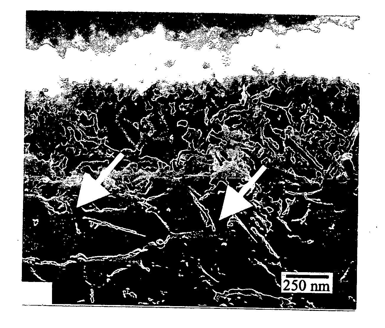
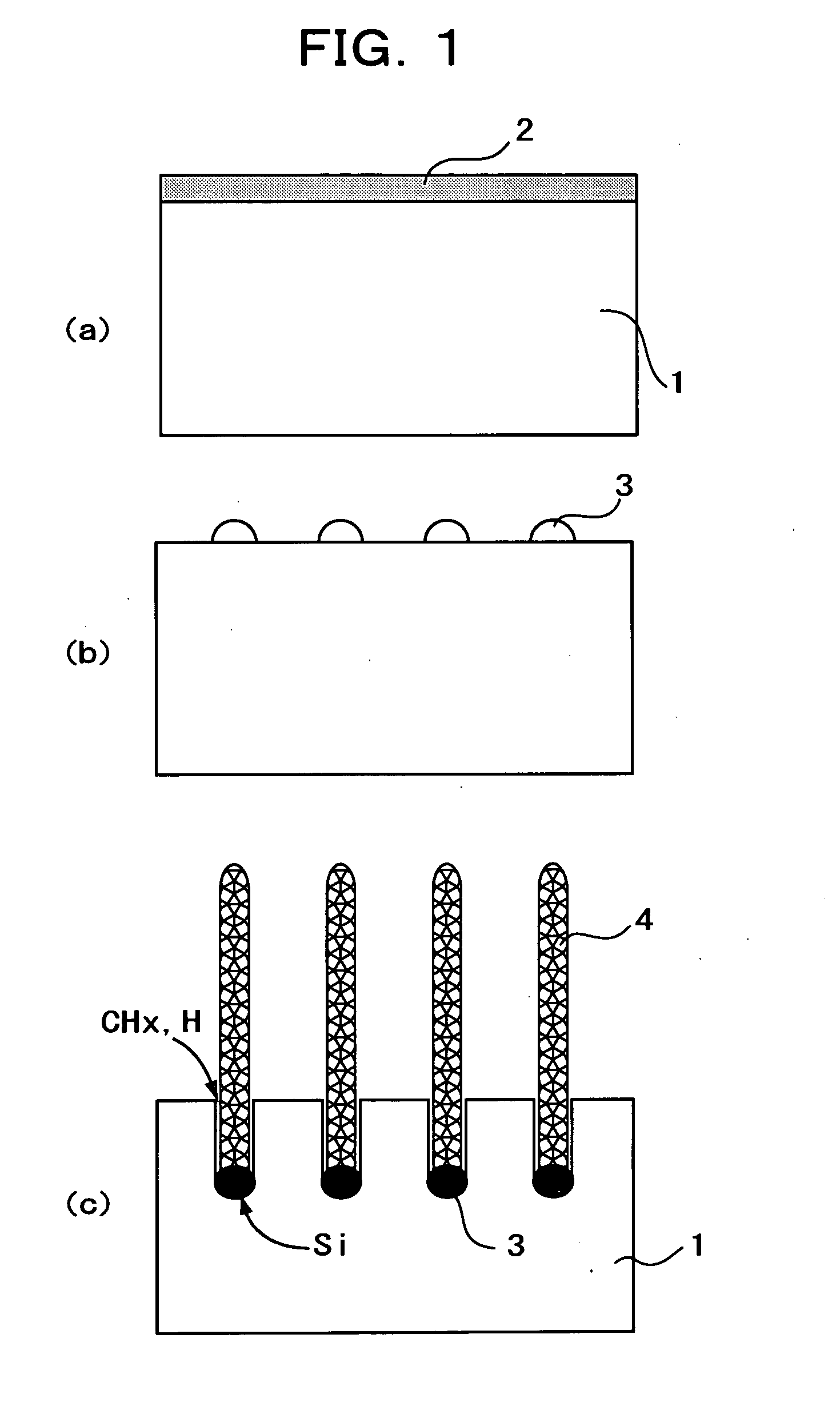
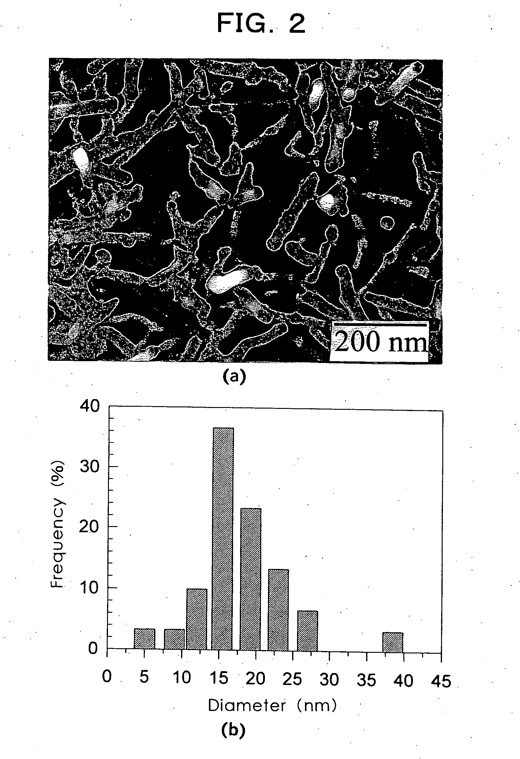
[0032] First, the synthesizing process of 3C—SiC nanowhisker according to the present invention is described. In the first process, Si substrate surface is cleaned with organic solvents and such acid as hydrofluoric acid. In the second process, metal thin film is deposited on the cleaned Si substrate by means of such film-forming method as spattering. In this process the thickness of the metal thin film is chosen depending on the aimed diameter of the 3C—SiC nanowhisker. In the third process. the Si substrate with the metal thin film deposited thereon is set in plasma CVD apparatus, hydrogen and hydrocarbon gases are flown at predetermined flow rate, and plasma discharge is excited while predetermined pressure is being maintained. A controlling device for the substrate temperature may not necessarily be used, but it may...


PUM

PropertyMeasurementUnit
thicknessaaaaaaaaaa
thicknessaaaaaaaaaa
temperatureaaaaaaaaaa

Abstract

The present invention offers a synthesizing method of 3C—SiC: nanowhisker wherein its diameter anid length can be controlled, it can grow on Si substrate, and wherein said method is safe and its cost is low. and said whisker cart emit visible light of various wravelength. 3C—SiC nanowhisker is formed by depositing thin film (2) made of a metal element on Si substrate (1), placing this Si substrate (1) into a plasma GVD apparaturi and by holding it for predetermined time at predetermined substrate temperature in the plasma consisting of hydrogen and hydrocarbon. Si of Si substrate 1) and C in plasma dissolve at supersaturation into metal liquid particle (3), 3C—SiC nanowhisker (4) grows on the metal liquid particle (3), whisker surface is terminated with H so to maintain the diameter constant, and the metal liquid particle (3) at whisker root takes in Si from Si substrate (1) and penetrates into Si substrate (1). This 3C—SiC nanowhicker cani be used as light-emitting material suitable to Si process, and 3C—SiC nanowhisker device which can emit light boased on quantum confinement effect and Si device can, if mixed together, form very useful device.

Description

TECHNICAL FIELD [0001] The present invention relates to 3C—SiC nanowhisker and nanowhiskers, having cubic lattice, nanometer size diameter, and chemical formula SiC, and relates to the synthesizing method of the same. PRIOR ART [0002] Crystalline materials having a size of nanometer are well known such as nanotubes, nanorods, and nanowhiskers. Such crystalline materials of nanometer size have specific geometrical and structural characteristics, therefore, for examnple, carbon nanotube can be used as electric field emission type electron source, storage system of chemical species, and mechanical reinforcing material. [0003] As those crystalline materials of nanometer size are the materials of having such very microscopic dimension as nanometer, they show various quantum size effects which bulky materials can not show. If those crystalline materials of nanometer size can be synthesized with their sizes controlled, their quantum effect can be controlled and then a nanoscale quantum dev...

Claims


Application Information

Patent Timeline
Patent Type & Authority Applications(United States)
IPC IPC(8): B82B1/00B82B3/00C01B31/36C30B11/00C30B25/00C30B25/10C30B29/62
CPCB82Y30/00Y10S423/10C01P2002/72C01P2002/80C01P2004/04C01P2004/16C01P2004/51C01P2004/64C30B11/00C30B25/005C30B25/105C01B31/36Y10T428/2993Y10T428/259C30B29/605C30B29/62C30B29/36C01B32/956C01B32/984
Inventor ANDO, TOSHIHIROGAMO, MIKA
Owner JAPAN SCI & TECH CORP
Why Eureka
Try Eureka