Method for fabricating transistor of semiconductor device

a semiconductor device and transistor technology, applied in semiconductor/solid-state device manufacturing, basic electric elements, electric devices, etc., can solve the problems of degrading the electrical characteristics of the drain region, increasing the hot carrier effect, and affecting the efficiency of the short channel effect, so as to achieve the effect of efficiently controlling the short channel effect and low source/drain resistance and gate resistan

Active Publication Date: 2005-04-28
MARVELL ASIA PTE LTD
View PDF22 Cites 13 Cited by
  • Summary
  • Abstract
  • Description
  • Claims
  • Application Information

AI Technical Summary

Benefits of technology

[0014] The present invention provides a method for fabricating a transistor device which can lower source / drain resistance and gate resistance without any additional process by forming a trench type gate and can efficiently control a short channel effect.

Problems solved by technology

As a consequence, hot carrier effect occurs inside a transistor and degrades electrical characteristics of a drain region, because the horizontal electric field is largely concentrated at the drain region when the channel length of the transistor is shorter relative to an external voltage applied.
Moreover, holes move out of the channel toward a substrate, while electrons are trapped under a gate oxide layer or spacers and affect the threshold voltage.
Therefore, the electric field in the channel is getting higher, with the result that the hot carrier effect becomes more severe.
However, the transistor with an LDD structure causes a short channel effect since the channel length gets continuously shorter due to the high integration of the semiconductor device.
Then, dopants in the LDD region diffuse to the channel and high electric field is applied in the channel edge between drains, which causes the hot carrier effect that degrades performance of the transistor.
Further, in operation of the transistor, impurities in source and drain regions diffuse laterally and the transistor may suffer from a punch-through effect easily.
Also, control of the threshold voltage is difficult when the channel length and the density control are not accurate.
However, this art also causes some problems in the miniaturization of the device since the gate is still higher than the silicon substrate because only part of the gate is buried in the substrate.
However, they require an additional mask process in forming the source / drain region, so the fabrication process is complicated.
This results in formation of a channel of the trench MOSFET device.
However, in the these patents, the miniaturization of the device is limited because the separation of the source / drain regions and fabrication processes are complicated.

Method used


Image

  • Method for fabricating transistor of semiconductor device
  • Method for fabricating transistor of semiconductor device
  • Method for fabricating transistor of semiconductor device

Examples


second embodiment

[0035]FIGS. 3a through 3g illustrate a manufacturing process of a transistor according to the present invention.

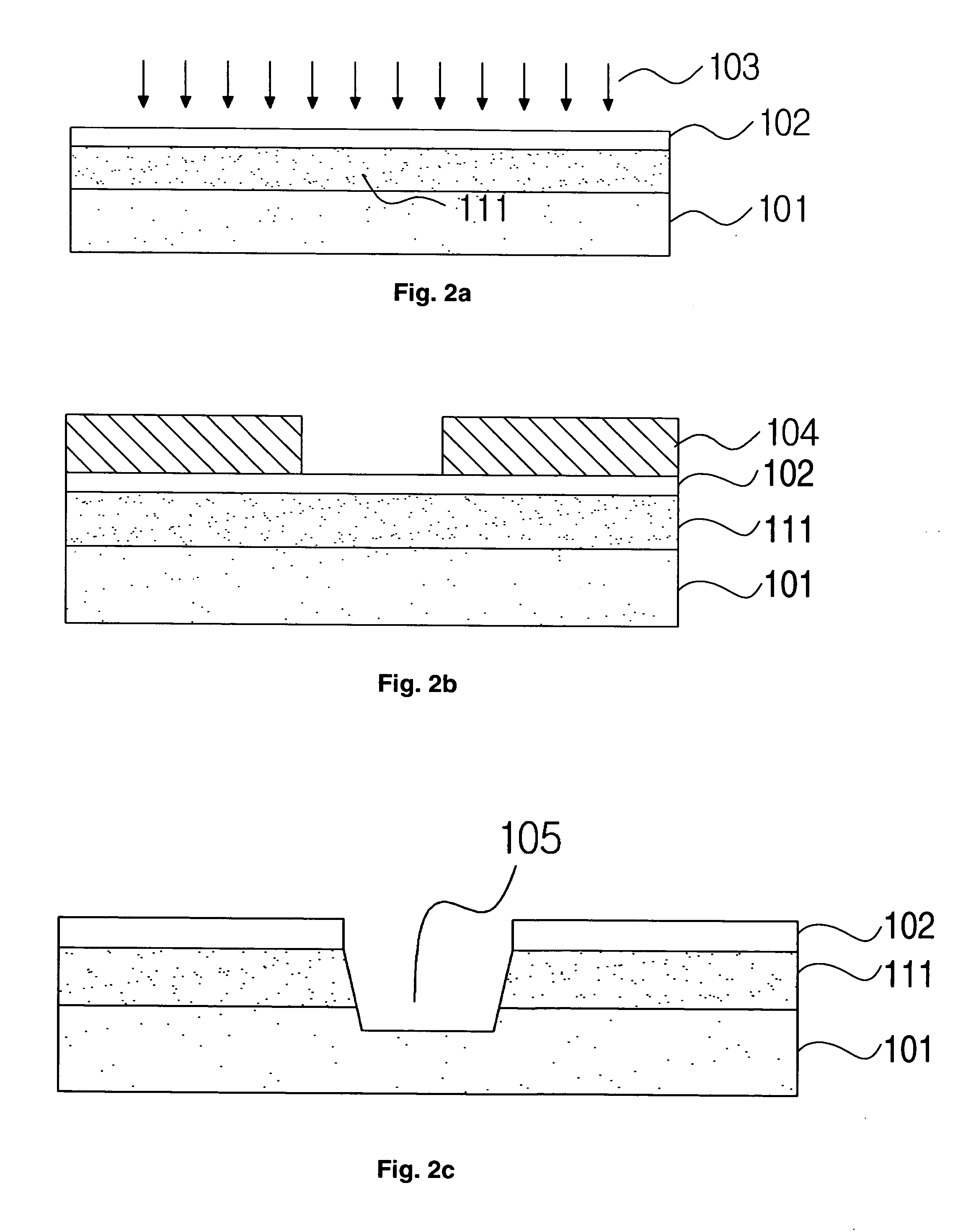
[0036] Referring to FIG. 3a, an LDD region 311 is formed on a silicon substrate 301 using an ion implantation 302. For a conventional transistor with a gate on a silicon substrate, a gate is formed first, and an LDD region is formed by an ion implantation process of impurities of low concentration using the gate as a mask. According to the present invention, the LDD region 311 is formed by the ion implantation process of impurities of low concentration prior to the formation of a gate. In one aspect, the ion implantation energy to form the LDD region 311 is between 10 keV and 80 keV.

[0037] Referring to FIG. 3b, a first insulating layer 303 is formed on the substrate and a photoresist pattern 304 is formed on the first insulating layer 303. The first insulating layer 303 is deposited on the substrate on which the LDD region 311 is already formed. The photoresist pattern 30...

third embodiment

[0044]FIGS. 4a through 4g illustrate a manufacturing method of a transistor according to the present invention.

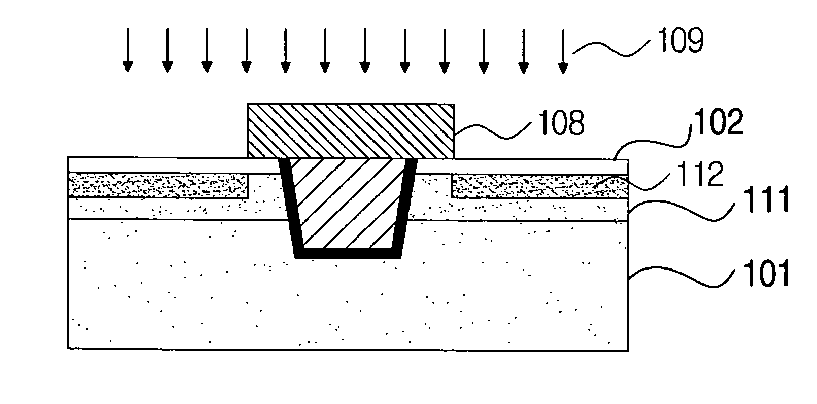
[0045] First, referring to FIG. 4a, a first insulating layer 502 is deposited on a silicon substrate 501 and an LDD region 511 is formed using ion implantation 503. The first insulating layer 502 works as a buffer layer for the ion implantation and may comprise a nitride layer deposited to a thickness between 500 Å and 1500 Å. In one aspect, the energy of the ion implantation for forming the LDD region 511 preferably is between 5 keV and 60 keV.

[0046] Referring to FIG. 4b, a first photoresist pattern 504 is formed on the first insulating layer 502 and then patterned to expose an area for the gate of the transistor with development and lithography processes.

[0047] Referring to FIG. 4c, a trench 505 is formed by etching the first insulating layer and the substrate using the first photoresist pattern 504 as a mask. Then, the first photoresist pattern 504 is removed. In one a...


PUM


Abstract

A method for fabricating a semiconductor transistor including forming a first insulating layer on a semiconductor substrate; forming an LDD region using ion implantation; patterning the first insulating layer; forming a trench in the substrate; forming a trench gate by depositing and planarizing a second insulating layer and a conductor on the substrate with the trench formed therein; forming a photoresist pattern on the substrate; forming source / drain regions by performing an ion implantation using the photoresist pattern as a mask; and removing the photoresist pattern and the first insulating layer. Thus, a method for fabricating a semiconductor transistor according to the present invention can reduce source / drain resistances and gate resistance by forming a trench type gate and can efficiently control a short channel effect.

Description

BACKGROUND OF THE INVENTION [0001] 1. Field of the Invention [0002] The present invention relates to a method for fabricating a transistor of a semiconductor device and, more particularly, to a method for fabricating a transistor which can lower source / drain resistance and gate resistance without any additional process by forming a trench type gate and can efficiently control a short channel effect. [0003] 2. Background of the Related Art [0004] Nowadays, width of a transistor gets continuously finer due to miniaturization and high integration of semiconductor. As a consequence, hot carrier effect occurs inside a transistor and degrades electrical characteristics of a drain region, because the horizontal electric field is largely concentrated at the drain region when the channel length of the transistor is shorter relative to an external voltage applied. Moreover, holes move out of the channel toward a substrate, while electrons are trapped under a gate oxide layer or spacers and af...

Claims


Application Information

Patent Timeline
Patent Type & Authority Applications(United States)
IPC IPC(8): H01L29/423H01L21/265H01L21/336H01L29/49H01L29/78
CPCH01L29/7834H01L29/66621
Inventor PARK, JEONG HO
Owner MARVELL ASIA PTE LTD
Why Eureka
Try Eureka