High density microvia substrate with high wireability

a microvia substrate and high-density technology, applied in the direction of printed circuit aspects, printed circuit non-printed electric components, semiconductor/solid-state device details, etc., can solve the problems of difficult to construct mutually segregated conductors to connect carrier lines to each terminal, lines with terminals, and difficult to connect carrier terminals. and terminals. carrying terminals and lines are particularly burdensome, so as to achieve high-density pth

Inactive Publication Date: 2005-05-05
GLOBALFOUNDRIES INC
View PDF13 Cites 15 Cited by
  • Summary
  • Abstract
  • Description
  • Claims
  • Application Information

AI Technical Summary

Benefits of technology

[0009] In accordance with the present invention, increased PTH density is achieved in fiber based chip carriers without the risk of fiber induced shorting by off-setting PTHs in a hole jog pattern. Fiber based chip carrier substrates typically arrange the fibers in a matrix pattern where the fibers are woven orthogonal to one another in an X-Y direction. By offsetting alternate rows of PTHs, the distance between holes along the same strands of fibers is substantially increased. Such an arrangement allows for increasing PTH density without decreasing the PTH to PTH spacing along the same strands of fibers. Jog patterns can be obtained by rotating a conventional X-Y grid pattern of PTHs between approximately 15° and 60°, depending upon such factors as the spacing between PTHs, the diameter of PTHs and the desired separation between rows and columns of PTHs.
[0012] It is a further object of the present invention to provide a chip carrier with improved wireability.
[0013] It is yet a further object of the present invention to provide a chip carrier with increased PTH density.
[0016] It is still another object of the present invention to provide high density PTH fiber-based chip carriers without decreasing PTH to PTH space in the X-Y direction.

Problems solved by technology

As the terminal density of semiconductor chips and, particularly, the density of Input / Output (I / O) connections of chips increases with improved technology, the wireability of chip carriers becomes more problematic.
The density of terminals tightly clustered makes it difficult to construct mutually segregated conductors to connect carrier lines to each terminal.
Signal carrying terminals and lines are particularly burdensome since they must be segregated from each other as well as from power and ground lines.
The density constraints of the PTH's in the core limits the vertical interconnection capability between the front and back of the carrier.
For example, high density PTH arrangements can result in reliability failures along glass fibers, from one hole to another, when the holes are placed too close together.
The inability to interconnect a large number of signals from the front and back of a chip carrier because of PTH density constraints caused by reliability problems when PTHs are placed too close together, limits the ability to connect higher I / O count chips to a chip carrier or to interconnect such chips to a printed circuit board (PCB).
Shorting between PTHs in glass reinforced epoxy carriers has been attributed to the fact that the epoxy bond to glass fibers is fairly poor.
When PTHs are drilled in the core and plating chemicals are used to plate the PTHs, the poor bonding of epoxy to the glass fibers allows the plating chemicals to penetrate some distance along the fibers.
This penetration can result in electrical shorting between holes.

Method used


Image

  • High density microvia substrate with high wireability
  • High density microvia substrate with high wireability
  • High density microvia substrate with high wireability

Examples


Embodiment Construction

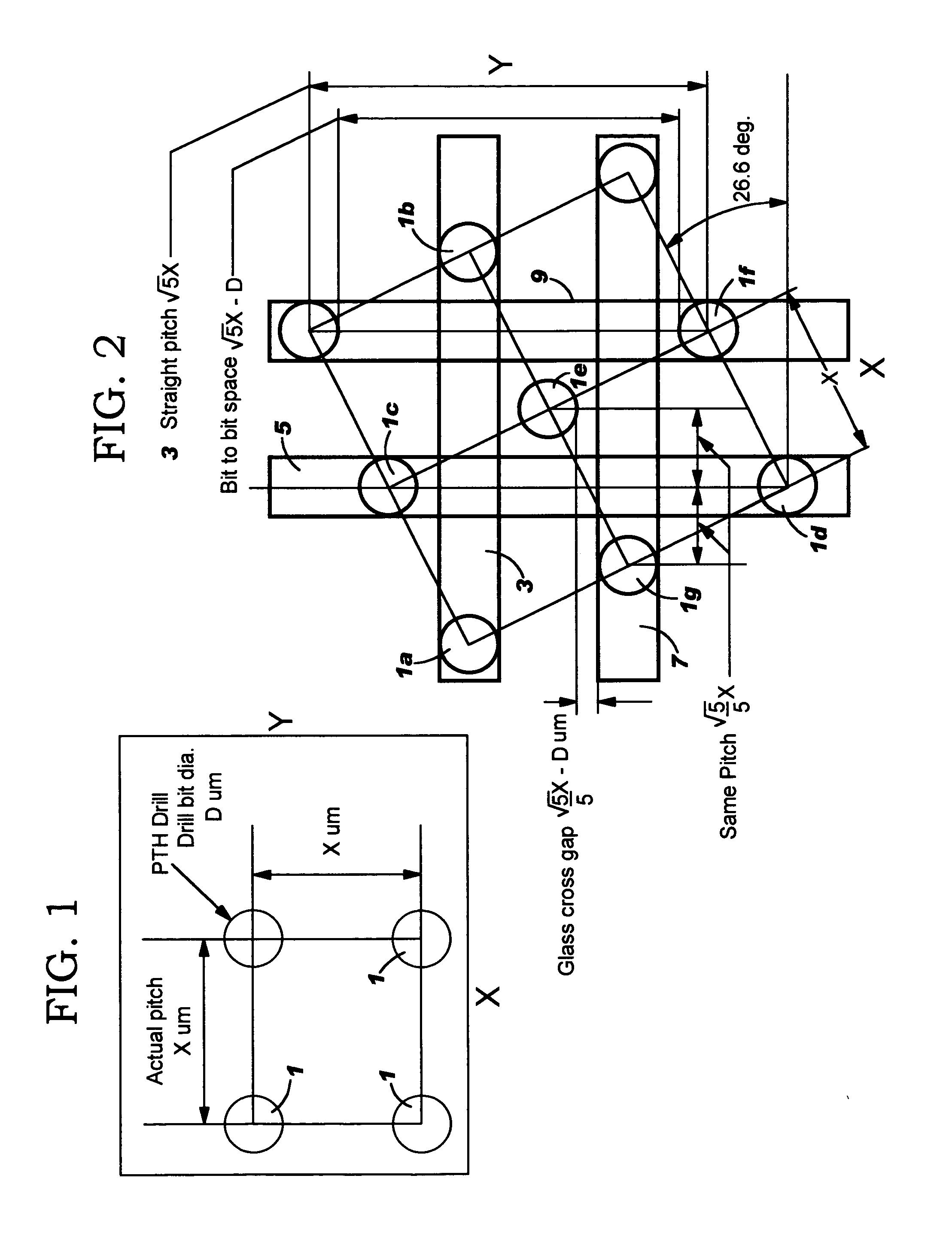
[0022] With reference to FIG. 1, there is shown a pattern of circles or holes 1 each representing a typical PTH with drill bit diameter Dim. Typically, the PTHs are plated to form a PTH grid arrangement. As shown, the holes 1 are arranged in an X-Y grid arrangement. In such arrangement, the X and Y lines of PTHs 1 are aligned with the direction of the glass fibers in the layers of the multilayer chip carrier. The fibers in the layers of such structure are typically woven m a mesh-like pattern with the fibers running parallel to one another and in both the X and Y direction generally intersecting orthogonally or at approximately at 90°. The actual pitch Xμm of holes is shown for both the X and Y directions. As used herein “orthogonal” means 90° or some minor variation one way or another.

[0023] The PTHs 1 in FIG. 1 would typically have a diameter of 150 μm and would be 300 μm or higher apart in both the X and Y direction. This results in a 450 μm or higher pitch which gives a density...


PUM

PropertyMeasurementUnit
angleaaaaaaaaaa
diameteraaaaaaaaaa
diameteraaaaaaaaaa

Abstract

The density of plated thru holes in a glass fiber based chip carrier is increased by off-setting holes to positions in which fibers from adjacent holes will not connect. Elongated strip zones or regions having a width approximately the diameter of the holes and running along orthogonal columns and rows of holes, parallel to the direction of fibers, define regions of fibers that can possibly cause shorting between holes. Rotating a conventional X-Y grid pattern of equidistant holes so as to position, for example, alternate holes in one direction between the elongated strip zones running in the opposite direction significantly increases the distance between holes along the elongated strip zones running in each direction. The holes are positioned between elongated strip zones with sufficient clearance to compensate for variations in the linear path of fibers.

Description

BACKGROUND OF THE INVENTION [0001]1. Field of the Invention [0002] The present invention relates to chip carriers and, more particularly, to high density chip carriers with high wireability for use with flip chip technology, and the like. [0003] 2. Background and Related Art [0004] As the terminal density of semiconductor chips and, particularly, the density of Input / Output (I / O) connections of chips increases with improved technology, the wireability of chip carriers becomes more problematic. The density of terminals tightly clustered makes it difficult to construct mutually segregated conductors to connect carrier lines to each terminal. Signal carrying terminals and lines are particularly burdensome since they must be segregated from each other as well as from power and ground lines. Signal lines on the chip carrier must have sufficient electrical isolation from other conductors so that undesired coupling and leakage paths are avoided. [0005] To enable routing in highly dense chi...

Claims


Application Information

Patent Timeline
Patent Type & Authority Applications(United States)
IPC IPC(8): H05K1/18H01L23/12H01L23/498H05K1/02H05K1/03H05K1/11H05K3/46
CPCH01L23/49822H05K2201/09627H01L2224/16H01L2924/0102H01L2924/01078H01L2924/15311H01L2924/3025H05K1/0366H05K1/112H05K1/115H05K3/4602H05K3/4626H05K2201/029H05K2201/09609H01L23/49838H05K1/02
Inventor KAWASAKI, KAZUSHIGEMEMIS, IRVING
Owner GLOBALFOUNDRIES INC
Why Eureka
Try Eureka