Differential amplifier circuit and multistage amplifier circuit

a technology of amplifier circuit and amplifier circuit, which is applied in the direction of differential amplifiers, amplifiers with semiconductor devices/discharge tubes, dc-amplifiers with dc-coupled stages, etc., can solve the adverse effect of analog circuit performance, frequency characteristics and jitters, and the curve of drain current vs. drain voltage is liable to show a kink, and achieve low jitter

Inactive Publication Date: 2005-05-05
MITSUBISHI ELECTRIC CORP
View PDF2 Cites 17 Cited by
  • Summary
  • Abstract
  • Description
  • Claims
  • Application Information

AI Technical Summary

Benefits of technology

[0040] According to the present invention, the first and second current control circuits are provided for both of the differential transistor pair and the gain compensation circuit is provided between the sources of the differential transistor pair, thereby eliminating AC kink effect at higher frequency due to such parasitic body resistance Rd and parasitic capacitance Cd as noted above. Consequently, approximately flat frequency characteristics can be attained at higher frequency, with jitters of pattern of output waveforms suppressed. BRIEF DESCRIPTION OF THE DRAWINGS

Problems solved by technology

In a field-effect transistor (FET) using SOI (Silicon On Insulator) process, since holes are easily accumulated inside a channel, a characteristics curve of drain current vs. drain voltage is liable to show a kink.
The parasitic body resistance Rd in SOI structure brings adverse effect on performances of analog circuits, e.g. frequency characteristics and jitters of output waveforms.
This effect becomes worse as sensitivity of buffer circuits becomes higher.

Method used


Image

  • Differential amplifier circuit and multistage amplifier circuit
  • Differential amplifier circuit and multistage amplifier circuit
  • Differential amplifier circuit and multistage amplifier circuit

Examples


embodiment 1

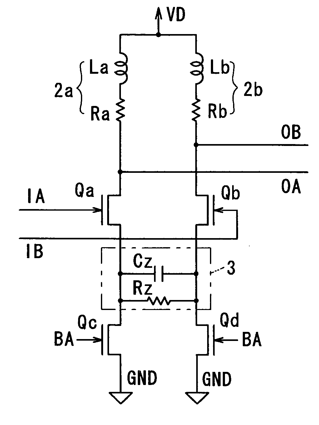
[0052]FIG. 1 is a circuit diagram showing the first embodiment of the present invention. A differential amplifier circuit includes a pair of field-effect transistors Qa and Qb, which can operate as differential transistor pair. The gate of the field-effect transistor Qa is supplied with an input signal IA for non-inverted input. The gate of the field-effect transistor Qb is supplied with an input signal IB for inverted input.

[0053] A load circuit 2a is connected between the drain of the field-effect transistor Qa and a power supply line VD. A load circuit 2b is connected between the drain of the field-effect transistor Qb and the power supply line VD. The load circuits 2a and 2b can be configured of various circuits, for example, herein series circuits of resistors Ra and Rb and inductors La and Lb, respectively.

[0054] Another field-effect transistor Qc is connected between the source of the field-effect transistor Qa and a ground line GND. Another field-effect transistor Qd is co...

embodiment 2

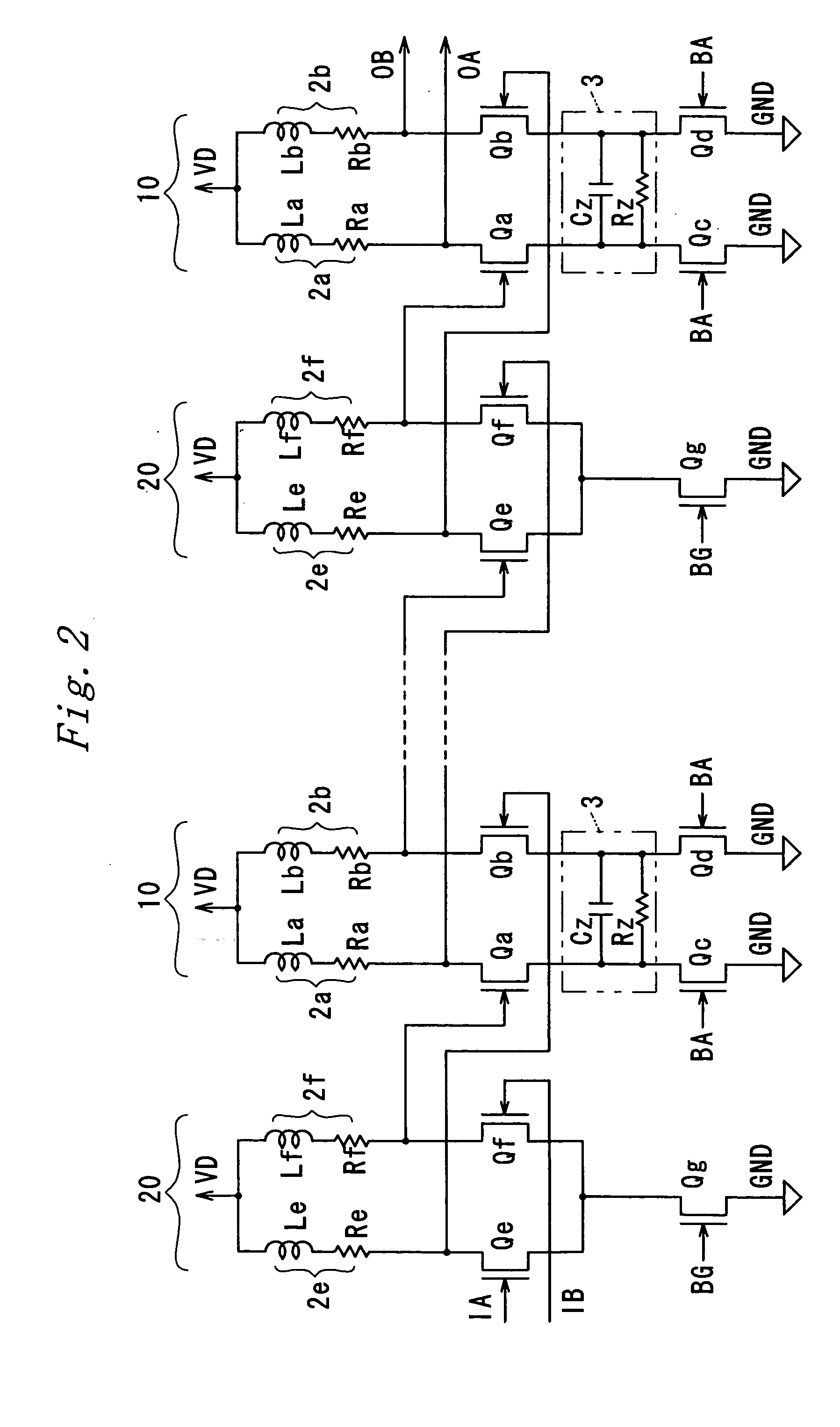
[0061]FIG. 2 is a circuit diagram showing the second embodiment of the present invention. A multistage amplifier circuit includes a differential amplifier circuit 10 according to the present invention and a general differential amplifier circuit 20, which are connected in multistage, for example, to constitute an input buffer in an analog circuit.

[0062] The differential amplifier circuit 10 includes, as shown in FIG. 1, the field-effect transistor Qa being operable base on a non-inverted input, the load circuit 2a which is connected to the drain of the field-effect transistor Qa, the field-effect transistor Qc for limiting current which is connected to the source of the field-effect transistor Qa, the field-effect transistor Qb being operable base on an inverted input; the load circuit 2b which is connected to the drain of the field-effect transistor Qb, the field-effect transistor Qd for limiting current which is connected to the source of the field-effect transistor Qb, and the g...

embodiment 3

[0073]FIG. 4 is a circuit diagram showing the third embodiment of the present invention, which exemplifies that capacitive diodes Cza and Czb, such as varactor or variable capacitance diode, are employed for the capacitor Cz of the gain compensation circuit 3.

[0074] A differential amplifier circuit includes a pair of field-effect transistors Qa and Qb, which can operate as differential transistor pair. The gate of the field-effect transistor Qa is supplied with an input signal IA for non-inverted input. The gate of the field-effect transistor Qb is supplied with an input signal IB for inverted input.

[0075] A load circuit 2a is connected between the drain of the field-effect transistor Qa and a power supply line VD. A load circuit 2b is connected between the drain of the field-effect transistor Qb and the power supply line VD. The load circuits 2a and 2b.can be configured of various circuits, for example, herein series circuits of resistors Ra and Rb and inductors La and Lb, respec...


PUM


Abstract

A differential amplifier circuit includes: a first field-effect transistor being operable base on a non-inverted input; a first load circuit which is connected to the drain of the first field-effect transistor; a first current control circuit which is connected to the source of the first field-effect transistor; a second field-effect transistor being operable base on an inverted input; a second load circuit which is connected to the drain of the second field-effect transistor; a second current control circuit which is connected to the source of the second field-effect transistor; and a gain compensation circuit which is connected between the source of the first field-effect transistor and the source of the second field-effect transistor, thereby attaining a high-speed differential amplifier circuit with low jitters.

Description

BACKGROUND OF THE INVENTION [0001] 1. Field of the Invention [0002] The present invention relates to a differential amplifier circuit and a multistage amplifier circuit using the same. [0003] 2. Description of the Related Art [0004] In a field-effect transistor (FET) using SOI (Silicon On Insulator) process, since holes are easily accumulated inside a channel, a characteristics curve of drain current vs. drain voltage is liable to show a kink. To avoid such a kink effect, fully depleted SOI process with a body contact is employed. In such SOI process, gates and contacts have parasitic body resistances relatively larger than those of C-MOS portions. [0005] On the other hand, since a transceiver input buffer circuit with high input sensitivity requires nearly 40 dB of total gain, generally differential transistor pairs which are connected in multistage cascade, as shown in FIG. 7A, are employed. [0006] In case the total body resistance becomes larger and a high gain is required, outpu...

Claims


Application Information

Patent Timeline
Patent Type & Authority Applications(United States)
IPC IPC(8): H03F3/45H03F3/68
CPCH03F3/45179H03F3/45197H03F2203/45458H03F2203/45466H03F2203/45702H03F2203/45496H03F2203/45638H03F2203/45652H03F2203/45472
Inventor CHEN, DANIEL YU-HUA
Owner MITSUBISHI ELECTRIC CORP
Why Eureka
Try Eureka