Film formation apparatus and film formation method and cleaning method

a film formation apparatus and film technology, applied in the direction of solid-state diffusion coating, plasma technique, vacuum evaporation coating, etc., can solve the problems of affecting the el layer deterioration, insufficient life of the element, and deterioration of the el layer, so as to prevent the dispersion of excited molecules of the dopant, the effect of enhancing the re-coupling efficiency of the carrier

Inactive Publication Date: 2005-05-19
SEMICON ENERGY LAB CO LTD
View PDF13 Cites 32 Cited by
  • Summary
  • Abstract
  • Description
  • Claims
  • Application Information

AI Technical Summary

Benefits of technology

[0026] In the above-mentioned respective film formation apparatuses, a plurality of deposition sources are arranged in one film formation chamber and in a single film formation chamber, a plurality of functional regions can be formed and thus a light emitting element having mixed regions can be formed. Accordingly, in the case an organic compound film comprising a plurality of functional regions is formed between an anode and a cathode of a light emitting element, unlike a conventional layered structure in which clear interfaces exist, a structure in which a mixed region of both of a material composing a first functional region and a material composing a second functional region is formed between the first functional region and the second functional region can be formed. In accordance with the invention, before the film formation or during the film formation, vacuum annealing is carried out, so that molecules in the mixed region can be fitted better with one another. Formation of the mixed region moderates the energy barrier between functional regions. Consequently, the driving voltage can be lowered and the deterioration of brightness can be prevented.
[0029] Further preferably, a light emitting region is composed of a host material and a light emitting material (a dopant) whose excitation energy is lower than that of the host material and the excitation energy of the dopant is planed to be lower than the excitation energy of a hole transporting region and the excitation energy of the electron transporting layer. Due to that, dispersion of excited molecules of a dopant can be prevented and the dopant can efficiently emit luminescence. Further, in the case a dopant is a carrier trap type material, the re-coupling efficiency of the carrier can be heightened.

Problems solved by technology

The most important problem of the EL element on practical application is that the life of the element is insufficient.
The deterioration of the element appears in a way that a non-light emitting region (a dark spot) is widened as the light emission is carried out for a long time and as a cause of the deterioration, the EL layer deterioration becomes an issue.
Further, it may be also possible that the deterioration of the EL layer is affected by contamination of the EL materials with other impurities.
In the case of film formation by a conventional deposition method, a deposition material is used as it is, but the deposition material for the deposition, is supposed to be contaminated with impurities.
Further, although the purity can be increased by previously refining the deposition material, there is probability that impurities are mixed by the time when evaporation is carried out.
EL materials are extremely susceptible to deterioration and easily oxidized and deteriorated in the presence of oxygen or water.
However, water or oxygen adsorbed in the deposition mask or the deposition preventing shield exposed to the atmospheric air may be probable to be isolated and taken in the film at the time of film formation using the organic EL materials and thus it is apprehended that adsorbed water or oxygen may be a factor of promoting deterioration of the organic EL materials.

Method used


Image

  • Film formation apparatus and film formation method and cleaning method
  • Film formation apparatus and film formation method and cleaning method
  • Film formation apparatus and film formation method and cleaning method

Examples


embodiment 1

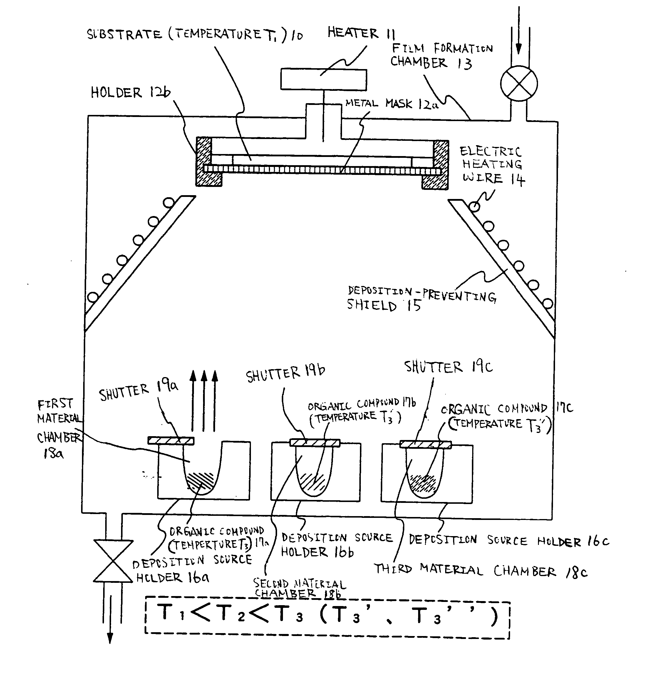
[0058] The constitution of a film formation apparatus of the invention will be described with reference to FIG. 1. FIG. 1 is one example of a cross-sectional view of the film formation apparatus of the invention.

[0059] At the time of forming a film by a deposition method, a face down method (referred to as a depositing-up method in some cases) is preferable and a substrate 10 is set in a manner that the face to form a film thereon is face down. The face down method is a method by which a film is formed while the face to form film of the substrate being kept face down and in such a method, adhesion of dust or the like can be suppressed.

[0060] As shown in FIG. 1, a heating means, in this case a heater 11, is installed adjacently to the substrate 10. By the heating means, the temperature (T1) of the substrate can be heated to 50 to 200° C., preferably 65 to 150° C. Further, a metal mask 12a fixed in a holder 12b is installed under the substrate 10 and deposition source holders 16a to...

embodiment 2

[0100] Here, a film formation apparatus different from that of the embodiment 1 is illustrated in FIG. 3.

[0101] As shown in FIG. 3, an example in which a heater furnace 31 and a cleaning preparatory chamber 22 are installed while being connected to a film formation chamber 33 will be described.

[0102] The heater furnace 31 for heating a substrate is made capable of carrying out annealing treatment by installing a heater in the outside. By the heater furnace 31, the temperature (T1) of the substrate is controlled to be 50 to 200° C., preferably 65 to 150° C. Further, a gate or a shutter shown as a dotted line in FIG. 3 is installed between the heater furnace 31 and the film formation chamber 33. Although it is not illustrated, a vacuum evacuation means may be additionally installed in the heater furnace 31. In this embodiment, after annealing is carried out in vacuum by the heater furnace 31 before deposition, the deposition is carried out by opening the gate.

[0103] Further, laser ...

embodiment 3

[0114] The constitution of another film formation apparatus of the invention will be described with the reference to FIG. 13. FIG. 13 shows an example of a cross-sectional view of another film formation apparatus of the invention.

[0115] As shown in FIG. 13, an example in which plasma 1301 is generated between a deposition mask 1302a connected to a high frequency power source 1300a through a capacitor 1300b and an electrode 1302b will be described.

[0116] The deposition mask 1302a fixed in a holder is installed adjacently to the portion (the portion shown by the dotted line in the figure) where a substrate is to be installed and a deposition source holder 1306 capable of heating at respective temperature is installed under it. A deposition source is installed on the opposite to the substrate.

[0117] Further, a material chamber 1308 is a space of the deposition source holder 1306 made of a conductive metal material and when the organic compound 1307 in the inside is heated to the sub...


PUM

PropertyMeasurementUnit
pressureaaaaaaaaaa
temperature T1aaaaaaaaaa
temperatureaaaaaaaaaa

Abstract

The purpose of the invention is to provide a film formation apparatus capable of forming an EL layer with a high purity and a high density, and a cleaning method. The invention is a formation of an EL layer with a high density by heating a substrate 10 by a heating means for heating a substrate, decreasing the pressure of a film formation chamber with a pressure decreasing means (a vacuum pump such as a turbo-molecular pump, a dry pump, or a cryopump) connected to the film formation chamber to 5×10⁻³ Torr (0.665 Pa) or lower, preferably 1×10⁻³ Torr (0.133 Pa) or lower, and carrying out film formation by depositing organic compound materials from deposition sources. In the film formation chamber, cleaning of deposition masks is carried out by plasma.

Description

BACKGROUND OF THE INVENTION [0001] 1. Field of the invention [0002] The present invention relates to a film formation apparatus and a film formation method employed for film formation of a film formable material (hereinafter, referred to as a deposition material) by deposition. Additionally, the invention relates to a cleaning method for removing a deposition material adhering to the inner wall or the like by the deposition. Particularly, the invention is an efficient technique in the case an organic material is used as the deposition material. [0003] 2. Related Art [0004] In recent years, investigations of light emitting apparatuses comprising EL elements as self-luminous type elements have been enthusiastically carried out and specially, light emitting apparatuses using organic materials as EL materials have drawn attention. Such a light emitting apparatus is called as an organic EL display (OELD) or an organic light emitting diode (OLED). [0005] The EL element comprises a layer (...

Claims


Application Information

Patent Timeline
Patent Type & Authority Applications(United States)
IPC IPC(8): C23C14/04C23C14/12C23C14/56H01L21/20C23C14/58
CPCB05D1/60C23C14/042C23C14/12C23C14/56C23C14/564Y10S438/905C23C14/5806C23C16/45514H01L51/001H01L51/5008H01L51/56C23C14/568C23F4/00H10K71/164H10K30/865H10K71/00H01L21/20
Inventor YAMAZAKI, SHUNPEIMURAKAMI, MASAKAZU
Owner SEMICON ENERGY LAB CO LTD
Why Eureka
Try Eureka