Method and apparatus for detecting electrostatic charges during semiconductor fabrication process

a technology of electrostatic charges and semiconductors, applied in the direction of electronic circuit testing, measurement devices, instruments, etc., can solve the problems of affecting the performance of semiconductor devices, and causing undesirable problems, etc., to achieve the effect of a rinsing process, reduce the physical dimensions of semiconductor devices, and high electric and corrosion resistan

Inactive Publication Date: 2005-05-26
WINBOND ELECTRONICS CORP
View PDF6 Cites 9 Cited by
  • Summary
  • Abstract
  • Description
  • Claims
  • Application Information

AI Technical Summary

Benefits of technology

[0002] Rinsing is a very important step in semiconductor fabrication processes. Typically, the rinsing step is performed using ultra high quality pure water or de-ionized water. Conventionally, the effectiveness of a rinsing process is measured by detecting the presence of particles or surface impurities, or by forming a metal-oxide semiconductor (MOS) device on the original oxide layer to qualitatively measure the stress-resistance thereof.
[0003] If the rinsing water contains particles or other impurities, these foreign substances of course will be carried onto the wafer surface, causing damages of the wafer and resulting in yield problems. More recently, it was discovered by the inventor of the present invention that, even with ultra-pure de-ionized rinsing water, undesirable problems can also be created. More specifically, it was discovered by the inventor of the present invention that if abnormalities are present in the rinsing water delivery system, the friction between water and the water delivery system, which is typically made of dielectric materials with high electric and corrosional resistances such as PFA, PTFE, etc, can cause electrostatic charges to be generated. These electrostatic charges will be carried by the rinsing water onto the wafer surface. When the electrostatic charges accumulate to a certain level, they can cause a dielectric layer, on which the electrostatic charges accumulate, to rupture. This phenomenon is called “charge damage”. An operation that cause electrostatic charges to be penetrate into the dielectric layer is called a charge damage.
[0004] As there exists the ever-present demand on semiconductor manufacturers to continuously reduce the physical dimensions of semiconductor devices, the resistance against charge damages that can be expected from a semiconductor device also continues to decline. As a result, it becomes increasingly critical during semiconductor fabricating processes to be able to quickly detect the presence of electrostatic charges, perform a trouble-shooting diagnosis, and have the problems solved and process resumed, without causing interruptions in the fabricating process. In addition to the charges that can be carried by the rinsing water, electrostatic charge damages can also be caused by the laminar air flow in the clean room, physical touches by human bodies, high-energy ion plantations, etc. As the semiconductor manufacturers are under an enormous pressure to cut cost by improving process yields, it is equally important to be able to timely and inexpensively detect those electrostatic charges so as to assure a smooth operation of the fabrication process.
[0005]FIG. 1 is a flowchart diagram which shows the main steps of a conventional process for detecting the charges on a wafer surface. It requires, among other things, the steps of: (1) wet cleaning and forming a sacrificial oxide layer; (2) removing the sacrificial oxide layer; (3) forming a gate layer first by oxidation; (4) deposition of poly or metal on the gate layer; (5) defining the gate pattern; (6) poly or metal etching to form the gate layer; (7) damage annealing; (8) running a charge damage process; (9) gate break-down probe; and (10) discard wafers that show high charge damages. As it can be seen from FIG. 1 and the above discussion, the conventional process for detecting the charges on a wafer surface is time- and labor-consuming, and it causes interruptions in the production processes.
[0006] The primary object of the present invention is to develop an improved method which can be used to, cost-effectively and with only minimum process interruption, detect electrostatic charges following a de-ionized water rinsing step during the fabrication of semiconductor devices to remove particles and other impurities from a wafer surface. More specifically, the primary of the present invention is to develop an improved method, and an apparatus for carrying out the same, for use in the semiconductor industry, to cost-effectively and expeditiously detect electrostatic charges that may have accumulated on the surface of a semiconductor wafer following a rinsing step which uses pure water or de-ionized water, to remove particles, and / or other impurities. The method of the present invention allows high precision and high resolution scanning to be made, so that it can very quickly and accurately pinpoint the trouble spot and allow a trouble-shooting diagnosis to be expeditiously performed. Furthermore, the present invention involves a much simpler procedure than any of those in the prior art processes, and, as a result, it can be very cost-effectively implemented and will not cause major interruptions in the semiconductor fabrication operation.
[0011] (d) Determining area or areas on the wafer surface with correspondingly high electrostatic charge density.

Problems solved by technology

If the rinsing water contains particles or other impurities, these foreign substances of course will be carried onto the wafer surface, causing damages of the wafer and resulting in yield problems.
More recently, it was discovered by the inventor of the present invention that, even with ultra-pure de-ionized rinsing water, undesirable problems can also be created.
When the electrostatic charges accumulate to a certain level, they can cause a dielectric layer, on which the electrostatic charges accumulate, to rupture.
As there exists the ever-present demand on semiconductor manufacturers to continuously reduce the physical dimensions of semiconductor devices, the resistance against charge damages that can be expected from a semiconductor device also continues to decline.
In addition to the charges that can be carried by the rinsing water, electrostatic charge damages can also be caused by the laminar air flow in the clean room, physical touches by human bodies, high-energy ion plantations, etc.
As it can be seen from FIG. 1 and the above discussion, the conventional process for detecting the charges on a wafer surface is time- and labor-consuming, and it causes interruptions in the production processes.

Method used


Image

  • Method and apparatus for detecting electrostatic charges during semiconductor fabrication process
  • Method and apparatus for detecting electrostatic charges during semiconductor fabrication process
  • Method and apparatus for detecting electrostatic charges during semiconductor fabrication process

Examples


example 1

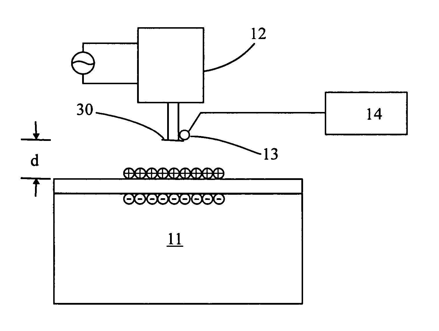
[0031]FIG. 2 shows a first preferred embodiment of the apparatus for carrying out the method of the present invention to detect electrostatic charges on a wafer surface.

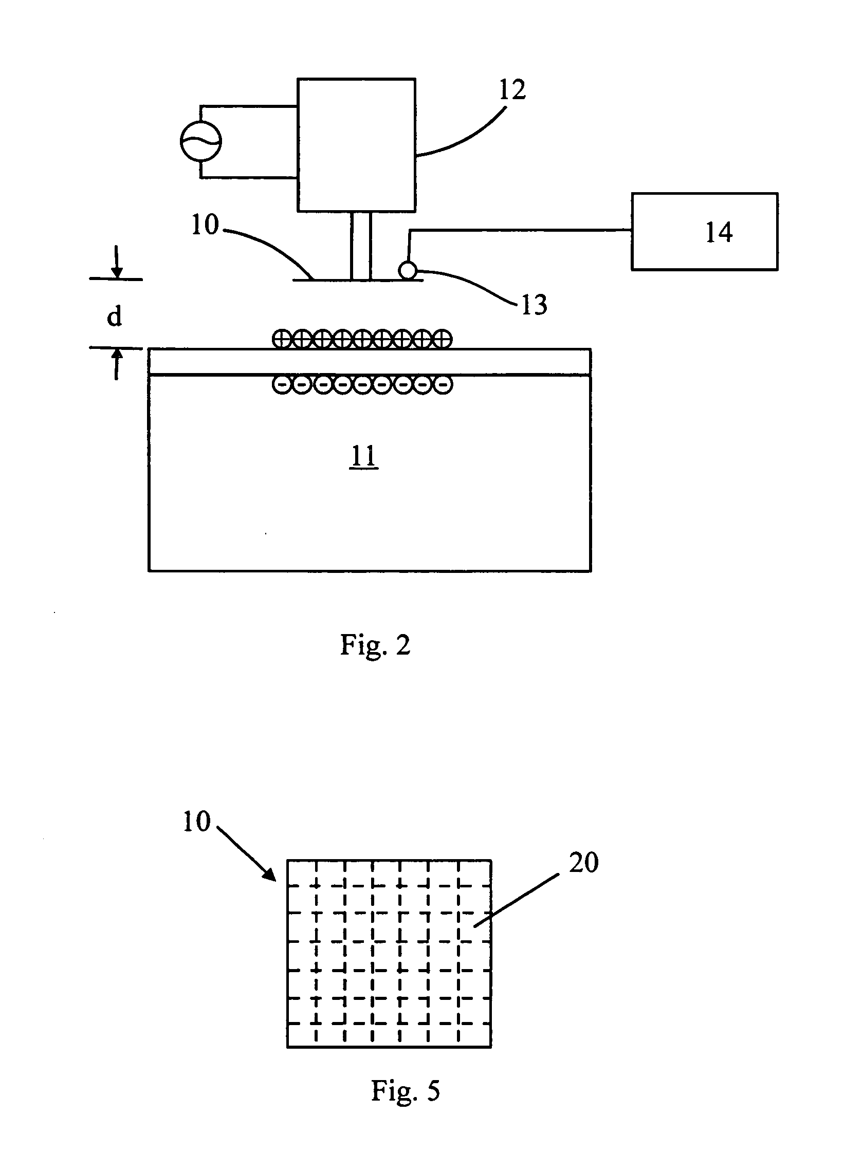
[0032] In FIG. 2, it is shown a capacitor plate 10 which is positioned above a wafer surface 11 on which a two-dimensional distribution of electrostatic charges is to be measured. The capacitor plate 10 is controlled by a mechanical vibrator 12, which causes the wafer 11 to move vertically as well as horizontally. A movable probe 13, which is connected to a Kelvin probe electronics 14, is utilized to measure (i.e., scanning) voltages at various locations at the capacitor plate 10.

[0033] After the capacitor plate 10 is moved by the mechanical vibrator 12 to a predetermined horizontal above the wafer surface with a predetermined distance separating the two, the movable probe 13 begins to scan over the capacitor plate 10 to obtain a two-dimensional voltage distribution at the capacitor plate 10. The measured voltage Δ...

example 2

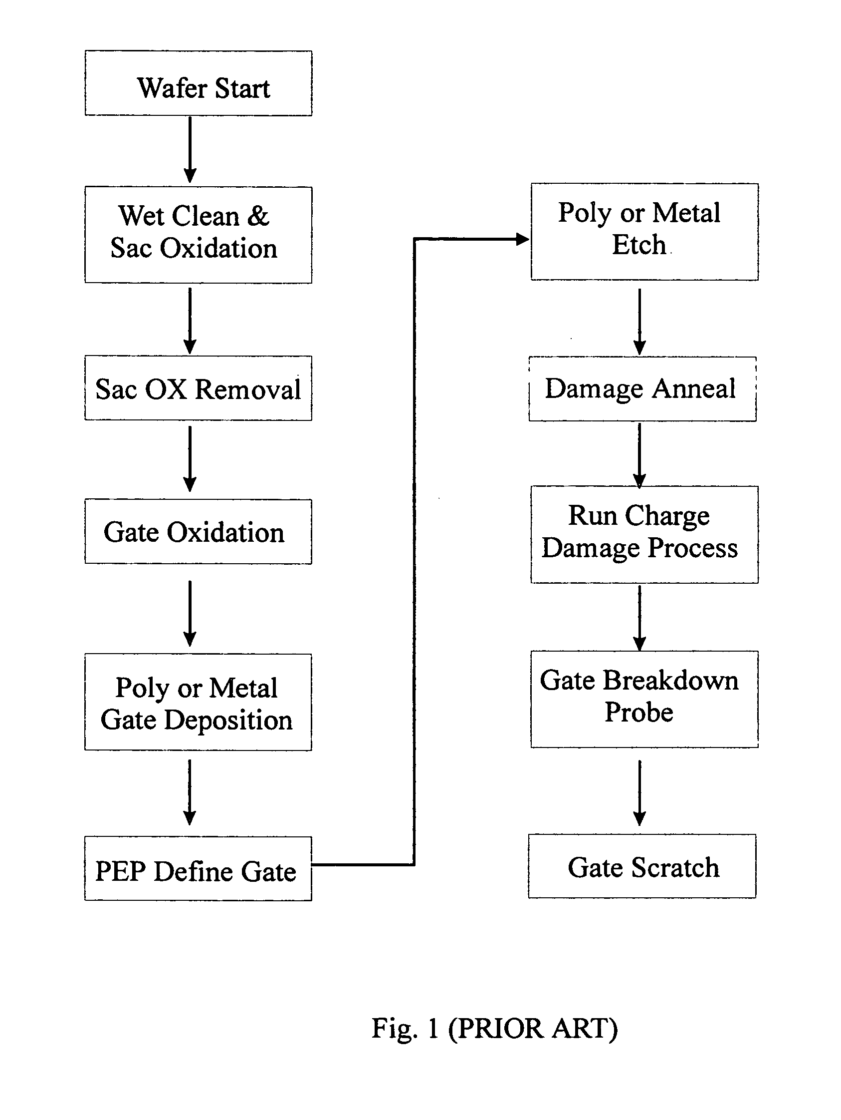
[0035]FIG. 3 is a schematic flowchart diagram showing the main steps of including the method of the present invention in a semiconductor device fabrication process. Compared to the conventional process as shown in FIG. 1, the method of the present invention is much more simplified. After an oxide layer is formed (Gate Oxidation), it is subject to a water rinsing step (Run Charge Damage Process). Thereafter, the steps described in Example 1 is performed (Wafer Surface Voltage Measurement). Since the method disclosed in the present invention does not require any additional physical contact with the wafer surface, the wafer fabrication process can be resumed without any interruption (Wafer Re-use, or Gate Oxide Removal).

[0036]FIG. 4A shows results obtained from a trouble-shooting test utilizing the method of the present invention. Initially, the accumulation of electrostatic charges was thought to be due to inadequate pressure of the de-ionized water. However, as shown in FIG. 4, incr...

example 3

[0037] In the second embodiment of the present invention, the apparatus is identical to that described in Example 1, except that the capacitor plate 10 is made of a plurality of isolated electrode sub-plates 20. This embodiment allows a better defined capacitor area to be employed for more quantitative results.


PUM


Abstract

A process for detecting electrostatic charges on a wafer surface during the fabrication of semiconductor devices after the wafer is subject to a de-ionized water rinsing step to remove particles and other impurities from a wafer surface. This process includes the steps of: (a) positioning an insulation layer above a wafer surface on which electrostatic charge densities are to be scanned; (b) using a movable probe to measure voltages at various locations at the insulating layer; (c) collecting the measured voltage distribution; and (d) examining the collected voltage distribution to identify areas on the wafer surface correspondingly to high electrostatic charge density. Because high precision and high resolution scanning can be made with this method, trouble-shooting diagnosis to be expeditiously performed with minimum interruptions to the semiconductor fabrication operation.

Description

FIELD OF THE INVENTION [0001] The present invention relates to a method which can be very used to detect electrostatic charges following a de-ionized water rinsing step during the fabrication of semiconductor devices to remove particles and other impurities from a wafer surface. More specifically, the present invention relates to a novel method, and an apparatus for carrying out the same, for use in the semiconductor industry, to conveniently and cost-effectively detect electrostatic charges that may be present on the surface of a semiconductor wafer following a rinsing step which uses pure water or de-ionized water, to remove particles, and / or other impurities. One of the most distinct advantages of the method of the present invention is that, because of its precision and high resolution, it can very quickly and accurately identify the troubled spot so as to allow a trouble-shooting diagnosis to be expeditiously performed. Another main advantage of the present invention is that, be...

Claims


Application Information

Patent Timeline
Patent Type & Authority Applications(United States)
IPC IPC(8): G01R29/24G01R31/28
CPCG01R31/2831G01R29/24
Inventor SHI, PENG-CHENG
Owner WINBOND ELECTRONICS CORP
Why Eureka
Try Eureka