

Undercoating layer material for lithography and wiring forming method using the same
a technology of undercoating layer and wiring, which is applied in the direction of photosensitive materials for photomechanical equipment, thin material processing, instruments, etc., can solve the problems of reducing the pattern resolution of the photoresist, requiring special equipment, and reducing the bonding or adhesion of the antireflection film to the substrate or resist film, etc., to achieve the effect of effective utilization of materials, less damage, and prolonged time and cumbersome operations
- Summary
- Abstract
- Description
- Claims
- Application Information
AI Technical Summary
Benefits of technology
Problems solved by technology
Method used
Image

Examples
examples
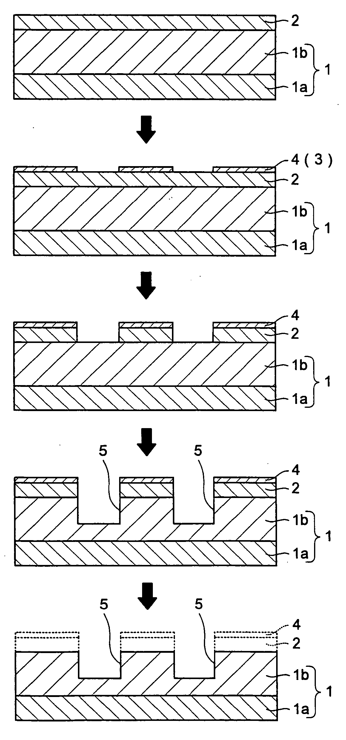
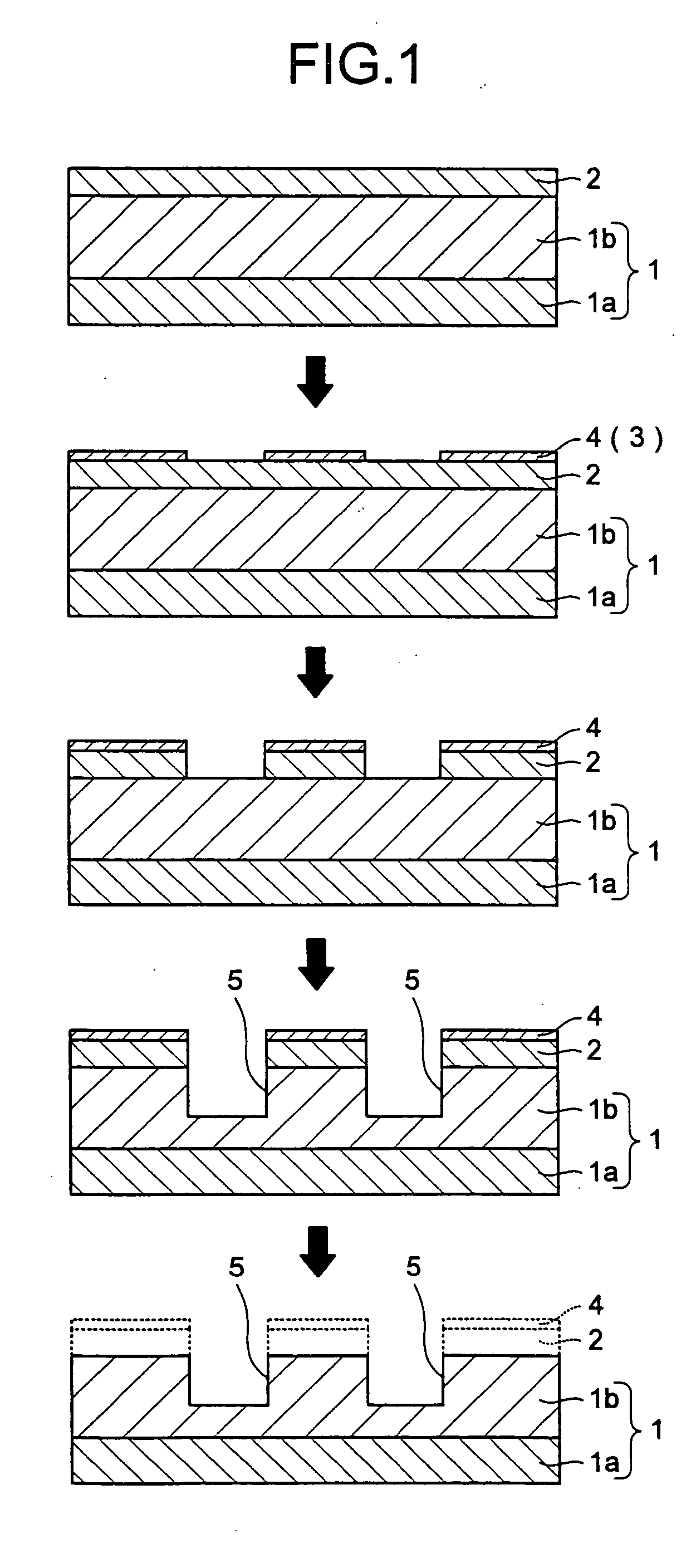
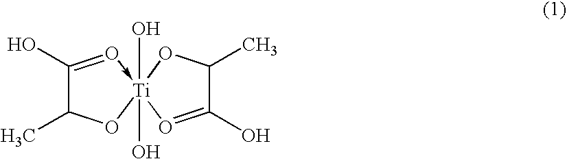
[0074] 24.05 g (0.2 mol) of dimethyidimethoxysilane, 81.75 g (0.6 mol) of methyltrimethoxysilane, 45.68 g (0.3 mol) of tetramethoxysilane, 117.75 g of isopropyl alcohol, 61.27 g of water, and 15.97 μl of an aqueous nitric acid solution (60% aqueous solution) were mixed together, and the resultant solution was stored at room tem perature (20° C.) for 3 hours, and then diluted with 205.56 g of isopropyl alcohol and 161.66 g of acetone to obtain a silane solution. To the silane solution were added 232.26 g of a titanium compound represented by formula (1) above (TC-310, manufactured by Matsumoto Chemical Industry, Co., Ltd.), 1447.07 g of isopropyl alcohol, and 762.67 g of acetone, to prepare an undercoating layer material.
[0075] A substrate having a 100-nm hole pattern (aspect ratio: 5) was then spin-coated with the undercoating layer material obtained in the above, and subjected to stepwise baking at 80° C. for 60 seconds, at 150° C. for 60 seconds, and at 260° C. for 180 seconds. T...
PUM
 Abstract
Description
Claims
Application Information