Method of fabricating a bipolar junction transistor

a bipolar junction transistor and transistor technology, applied in the field of bipolar junction transistor fabrication, can solve the problems of increasing the complexity of the total processing steps of the bjt, device damage, and device damage, so as to reduce the resistance of the collector, reduce the production cost, and simplify the processing steps

Inactive Publication Date: 2005-05-26
UNITED MICROELECTRONICS CORP
View PDF6 Cites 3 Cited by
  • Summary
  • Abstract
  • Description
  • Claims
  • Application Information

AI Technical Summary

Benefits of technology

[0013] It is an advantage of the present invention that the doping region formed in the substrate is used as a collector of the BJT. Therefore, the processing steps of forming the structures of the alignment marks, the buried doping region, the epitaxial layer, the collector and the channel stops as in the conventional BJT are not necessary in the present invention. As a result, the total number of masks for fabricating the BJT of the present invention can be effectively reduced, so as to simplify the processing steps and reduce the production costs. In comparison with the buried doping regions, the epitaxial layer and the collector of the conventional BJT, a shallower collector is formed in the present invention. Therefore, the resistance of the collector can be reduced and a better electrical performance can be provided by the BJT of the present invention. In addition, the present invention may further use the doping region as an emitter, and use the second doping layer as a collector of the BJT. In this case, the advantages of omitting the conventional steps of fabricating the buried doping region, the epitaxial layer, the collector and the channel stops can also be approached. The total number of masks for fabricating the BJT is therefore reduced to simplify the processing steps and reduce the production costs. Furthermore, the resistance of the collector can be reduced to provide a better electrical performance according to the present invention.
[0014] These and other objects of the claimed invention will be apparent to those of ordinary skill in the art after reading the following detailed description of the preferred embodiment that is illustrated in the various figures and drawings.

Problems solved by technology

Currently, multiple masking steps are used to combine sequences of the BJT fabrication steps and the CMOS transistor fabrication steps, which increasing complication of the total processing steps.
In this case, the total processing steps of the BJT become very complicated.
In addition, during the repeated masking steps, such as forming the masks and removing the masks, the device is possible damaged to have a bad electrical performance.

Method used


Image

  • Method of fabricating a bipolar junction transistor
  • Method of fabricating a bipolar junction transistor
  • Method of fabricating a bipolar junction transistor

Examples


first embodiment

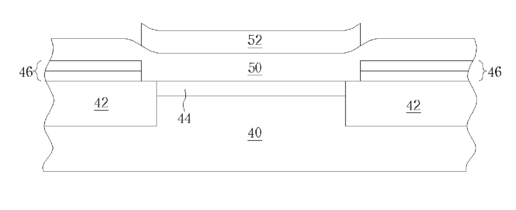
[0019] Referring to FIGS. 7-14, FIGS. 7-14 are schematic diagrams of a method of fabricating a BJT according to the present invention. Since the present method of fabricating the BJT can be optionally combined with processing steps of a CMOS transistor and the processing steps of the CMOS transistor are already well known by the current industry, FIGS. 7-14 are focused on illustrating the processing steps of the BJT only.

[0020] As shown in FIG. 7, a substrate 40 with a plurality of isolation structures 42 for defining at least an active area A on the substrate 40 is provided. The isolation structures 42 can be shallow trench isolation (STI) or field oxide layers. The substrate 40 can be a P-type silicon substrate. Then, an ion implantation process is performed, for example a doping process for forming a source / drain of an NMOS of a CMOS transistor on the substrate 40 is used together with a thermal treatment to form an N-type doping region 44 within the active area A. The N-type dop...

second embodiment

[0027] Referring to FIGS. 16-24, FIGS. 16-24 are schematic diagrams of a method of fabricating a BJT according to the present invention. Since the present method of fabricating the BJT can be optionally combined with processing steps of a CMOS transistor and the processing steps of the CMOS transistor are already well known by the current industry, FIGS. 16-24 are focused on illustrating the processing steps of the BJT only.

[0028] As shown in FIG. 16, a substrate 60 with a plurality of isolation structures 62 for defining at least an active area A on the substrate 60 is provided. The isolation structures 62 can be shallow trench isolation or field oxide layers. The substrate 60 can be a P-type silicon substrate. Then, an ion implantation process is performed, for example a doping process for forming a source / drain of an NMOS of a CMOS transistor on the substrate 60 is used together with a thermal treatment to form an N-type doping region 64 within the active area A. The N-type dopin...


PUM


Abstract

A substrate with a plurality of isolation structures for defining at least an active area thereon is provided. Ions of a first conductive type are implanted into the substrate to form a doping region in the active area. Following that, a protective layer is formed on the substrate, the protective layer having an opening to expose the doping region. A first doping layer of a second conductive type and a second doping layer of the first conductive type are formed on the doping region, respectively, to complete fabrication of a bipolar junction transistor.

Description

CROSS REFERENCE TO RELATED APPLICATIONS [0001] This application is a divisional of application Ser. No. 10 / 707,215 filed Nov. 26, 2003.BACKGROUND OF INVENTION [0002] 1. Field of the Invention [0003] The present invention relates to a method of fabricating a bipolar junction transistor (BJT), and more particularly, to a method of fabricating a vertical BJT. [0004] 2. Description of the Prior Art [0005] A BJT utilizes two types of carriers, “electrons” and “hot holes”, to transmit current. The BJT continues to be a basic circuit element in integrated circuits due to its high switching capability and current carrying capacity. A BiCMOS transistor is constructed by a particular combination of the BJT and a complementary metal oxide semiconductor (CMOS) transistor positioned on the same integrated circuit, so as to speed up an operation of the CMOS transistor. Currently, multiple masking steps are used to combine sequences of the BJT fabrication steps and the CMOS transistor fabrication ...

Claims


Application Information

Patent Timeline
Patent Type & Authority Applications(United States)
IPC IPC(8): H01L21/331H01L29/732
CPCH01L29/732H01L29/66287
Inventor GAU, JING-HORNG
Owner UNITED MICROELECTRONICS CORP
Why Eureka
Try Eureka