Integrated scheme for yield improvement by self-consistent minimization of IC design and process interactions

Inactive Publication Date: 2005-05-26
AXELRAD VALERY +2
View PDF0 Cites 31 Cited by
  • Summary
  • Abstract
  • Description
  • Claims
  • Application Information

AI Technical Summary

Benefits of technology

[0012] The present invention fills these needs by providing methods for improving the performance and yield of semiconductor ICs

Problems solved by technology

As a result, for small dimensions (e.g. sub 0.25 microns), advances are increasingly limited by this lack of pattern fidelity in a series of lithography and etch process steps.
All OPC systems increase mask complexity and thus cost of mask manufacturing which becomes a significant fraction of total semiconductor wafer processing cost.
This directly translates into increased cost of semiconductor integrated circuits.
Apart from increased manufacturing complexity and cost there is one major drawback with the current OPC implementations.
This drawback stems from the fact that current OPC implementations use the overall geometric accuracy of the pattern replication of lithography and

Method used


Image

  • Integrated scheme for yield improvement by self-consistent minimization of IC design and process interactions
  • Integrated scheme for yield improvement by self-consistent minimization of IC design and process interactions
  • Integrated scheme for yield improvement by self-consistent minimization of IC design and process interactions

Examples


Embodiment Construction

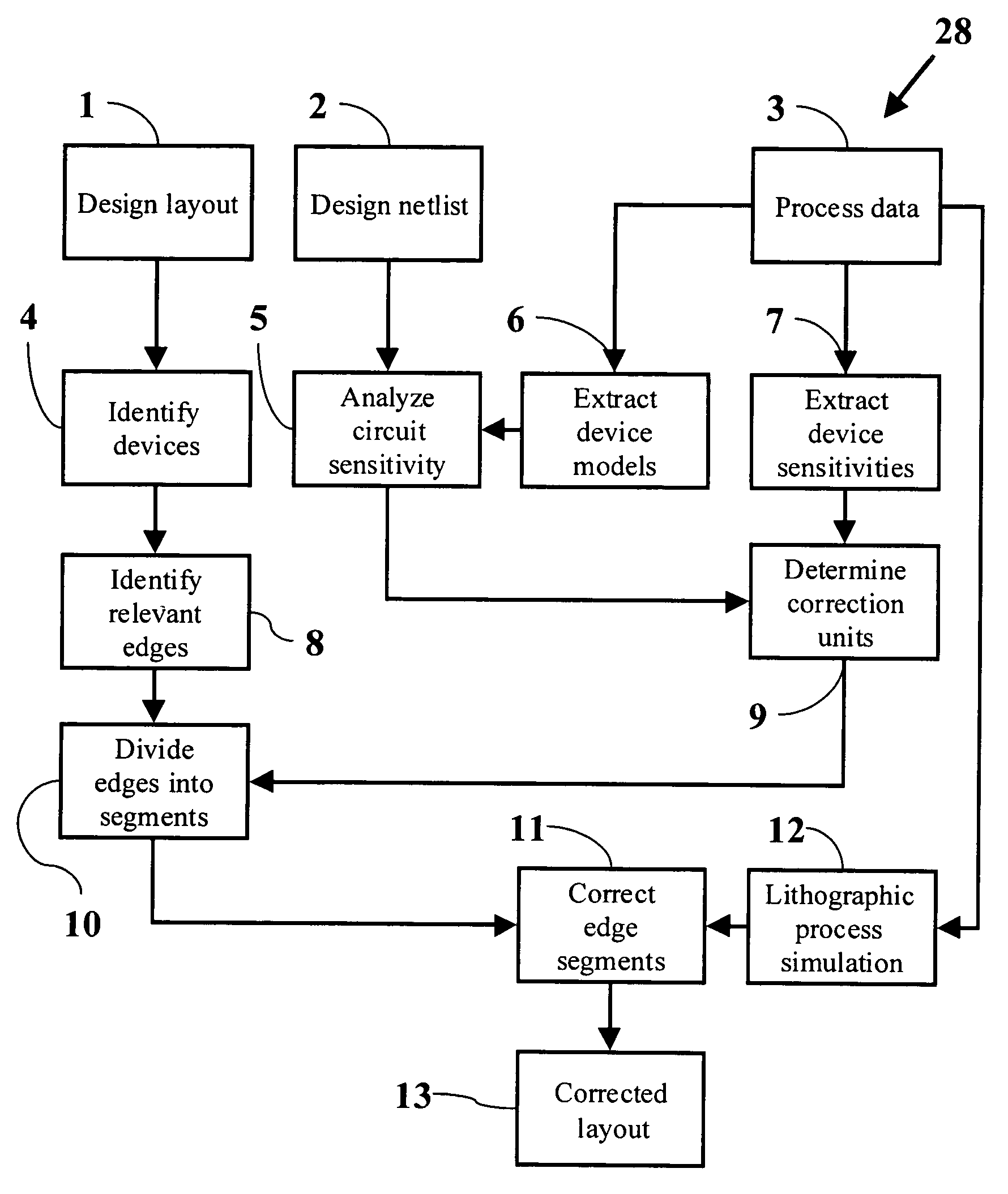
[0032] The present invention includes an integrated simulation scheme for yield improvement by self-consistent minimization of design and process interactions. Circuit sensitivity to device performance and device performance sensitivity to geometry distortions is analyzed using process-specific device models, thus capturing design-process interactions. Devices are then identified on layout and geometry distortion is predicted using lithographic process simulation. Layout corrections are subsequently applied only where it is required to meet circuit performance requirements.

[0033]FIG. 1 is a flow chart 28 of a method of the present invention. In this method, the design data comprising design layout 1 and design netlist 2 is used in combination with process data 3 to calculate corrections required to improve design yield.

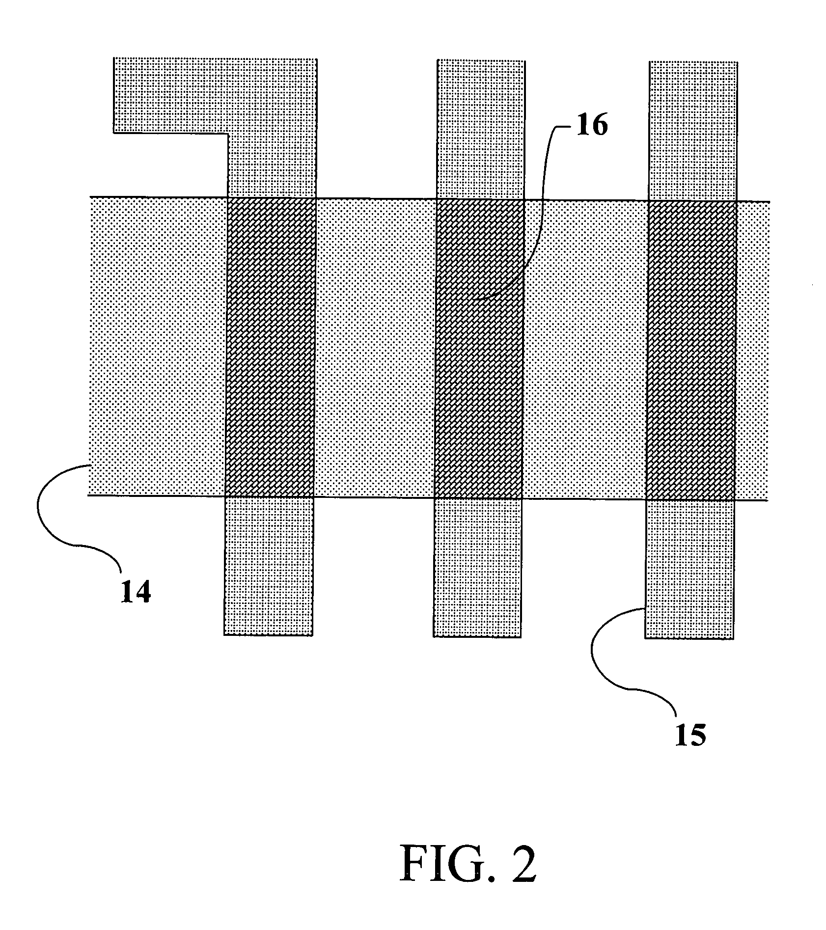
[0034] Device identification step 4 is illustrated in FIG. 2 and FIG. 3, active devices 16 are identified by performing boolean AND on poly 15 and active 14 layer m...


PUM


Abstract

A method for performing self-consistent minimization of IC design and process interactions is disclosed. This method is based on calculating the amount of design-process interaction based on the information derived from circuit sensitivity analysis and process characterization. Optical proximity correction is subsequently performed in such a way that a) ensures that desired circuit performance is achieved in a given manufacturing environment if at all possible and b) also limits the increase in mask complexity to a realistic minimum.

Description

CROSS REFERENCE TO RELATED APPLICATIONS [0001] This patent application is claiming the benefit of a prior filed provisional application Ser. No. 60 / 451,428, filed on Mar. 03, 2003, entitled “An Integrated Scheme for Yield Improvement by Self-Consistent Minimization of IC Design and Process Interactions”.BACKGROUND OF THE INVENTION [0002] 1. Field of the Invention [0003] The present invention generally relates to the manufacture of very large scale integrated (VLSI) circuit devices and, more particularly, to the improvement of manufacturability of VLSI circuits through the use of Process Proximity Correction (PPC) and Optical Proximity Correction (OPC). [0004] 2. Description of the Related Art [0005] Manufacturing of semiconductor devices is dependent upon the accurate replication of computer aided design (CAD) generated patterns onto the surface of a semiconductor substrate. The replication process is typically performed using optical lithography followed by a variety of subtractive...

Claims


Application Information

Patent Timeline
IPC IPC(8): G03F1/14G06F17/50
CPCG03F1/144G06F17/5068G03F1/36G06F30/39
Inventor AXELRAD, VALERYSHIBKOV, ANDREIBOKSHA, VICTOR VLADIMIR
Owner AXELRAD VALERY
Why Eureka
Try Eureka