

Semiconductor device and method for manufacturing the same
a technology of semiconductors and semiconductors, applied in the direction of transistors, optics, instruments, etc., can solve the problems of low effect of blocking impurity ions, varying the electric characteristics of tft, and internal stress, so as to improve the reliability of tft and eliminate internal stress
- Summary
- Abstract
- Description
- Claims
- Application Information
AI Technical Summary
Benefits of technology
Problems solved by technology
Method used
Image

Examples
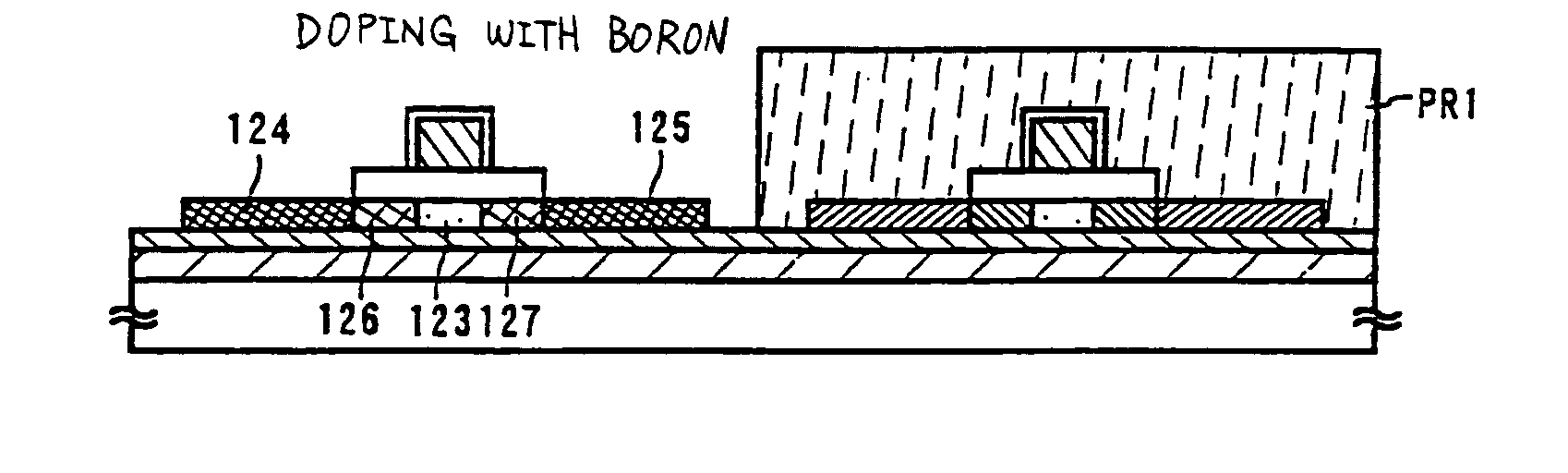
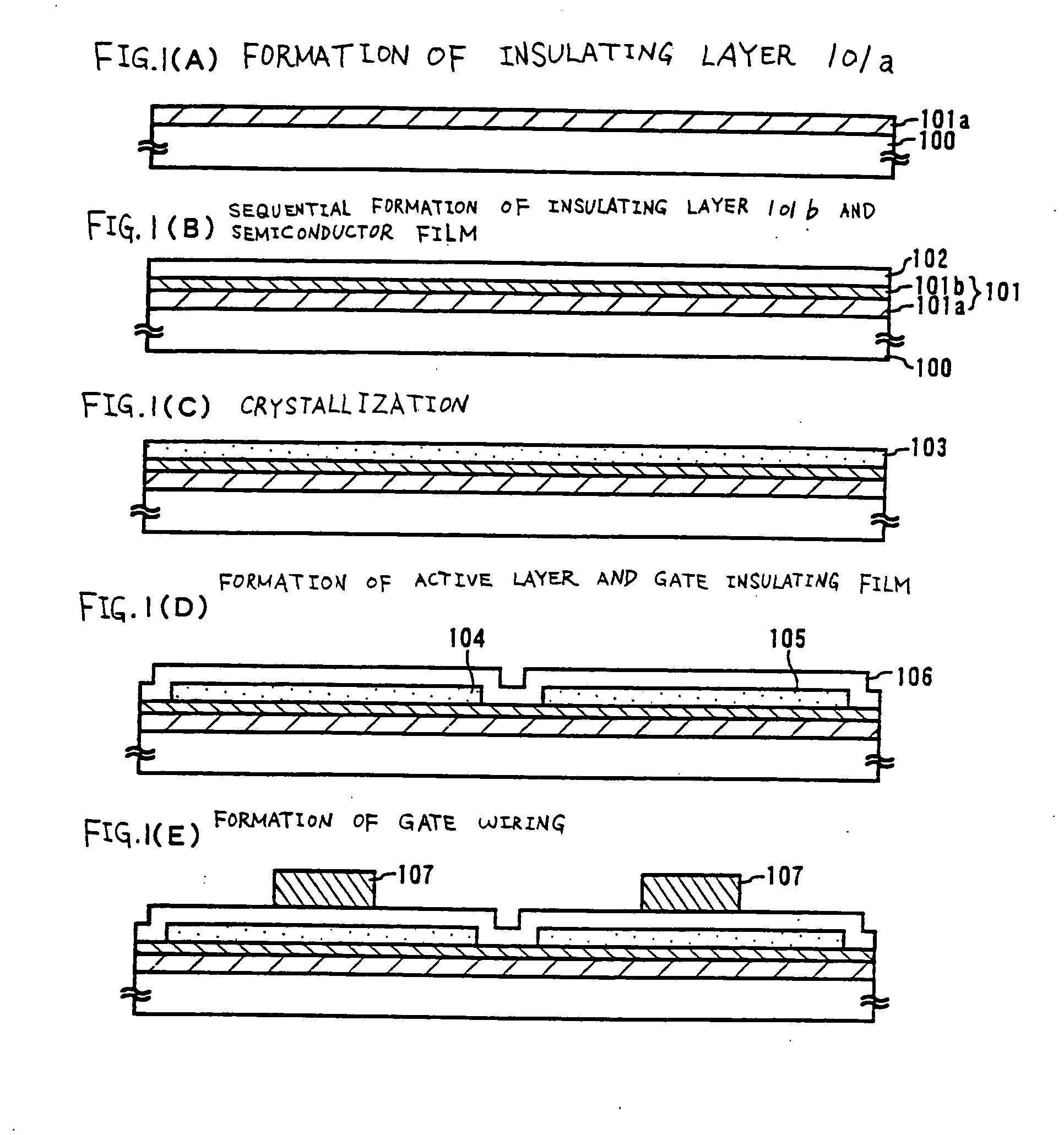
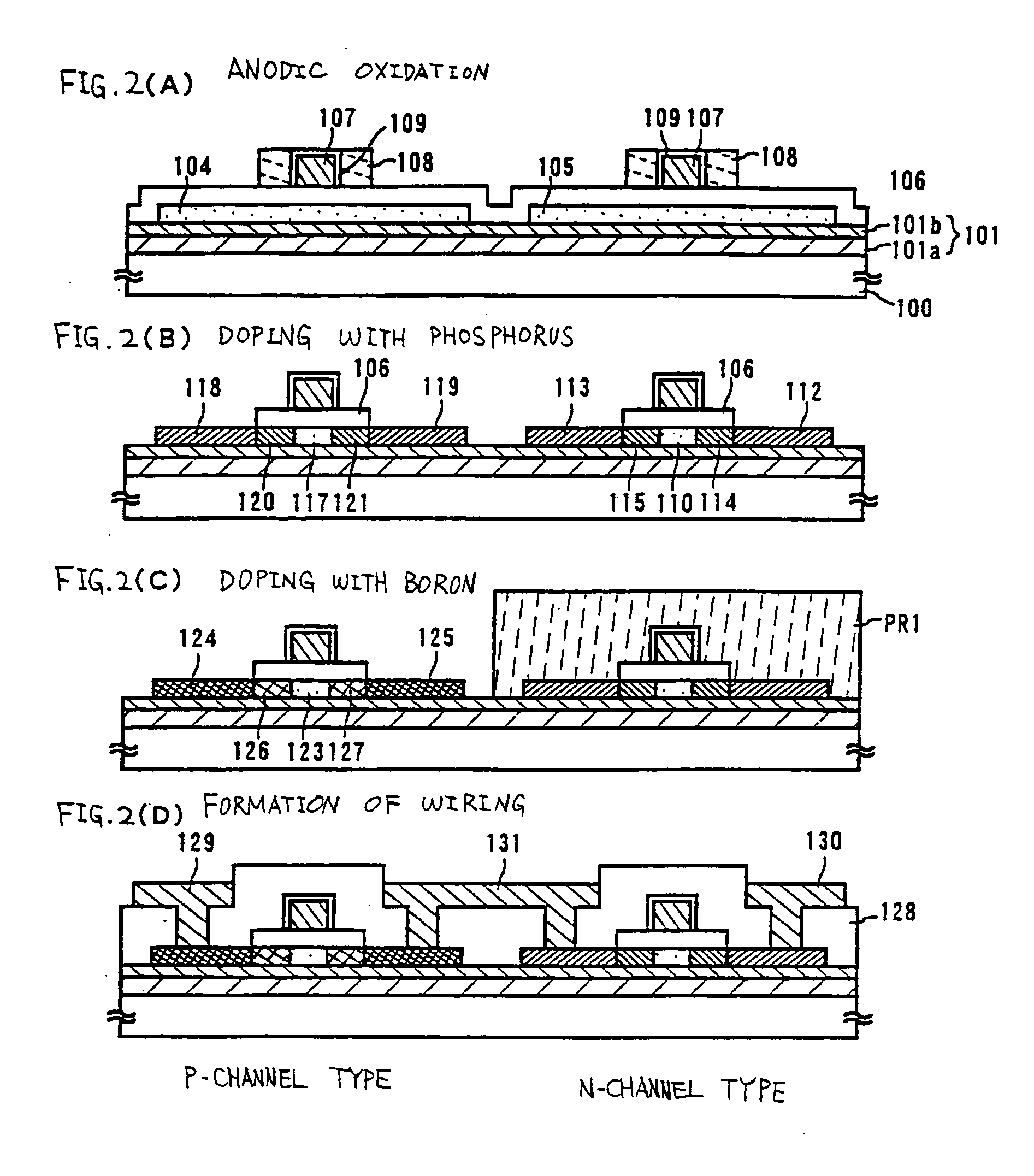
embodiment 1
[0105] In the present embodiment, there will be described an active-matrix-type liquid crystal panel in which a pixel matrix circuit is integrated with a driver circuit on the same substrate. Also, the structure of a TFT capable of effectively preventing the deterioration will be described in the present embodiment.
[0106] A liquid crystal display will schematically be illustrated in FIG. 11. An active matrix substrate is bonded to an opposite substrate with a gap between them and the gap is filled with liquid crystal.
[0107] An active matrix substrate 300 includes a pixel matrix circuit 301, a gate driver circuit 302, a source driver circuit 303, and a signal processing circuit 304, each of which is formed of a TFT made on the substrate. The gate driver circuit 302 and the source driver circuit 303 are used for driving the TFT of the pixel matrix circuit 301. The signal processing circuit 305 is a circuit for processing various kinds of signals required to display images and means ...
embodiment 2
[0143] In the present embodiment, an example of manufacturing an EL display device using the present invention will be described. In this connection, FIG. 12(A) is a plan view of an EL display device in accordance with the present invention and FIG. 12(B) is a cross-sectional view thereof.
[0144] In FIG. 12(A), a reference numeral 3001 designates a substrate, a reference numeral 3002 designates a pixel part, a reference numeral 3003 designates a source side driver circuit, and a reference numeral 3004 designates a gate side driver circuit, and each driver circuit leads to a FPC (flexible printed circuit) 3006 via a wiring 3005, and is connected to an external device.
[0145] Here, a first sealing member 3101, a covering member 3102, a filling material 3103 and a second sealing member 3104 are provided such that they surround the pixel part 3002, the source side driver circuit 3003, and the gate side driver circuit 3004.
[0146] Also, FIG. 12(B) corresponds to a cross-sectional view ta...
embodiment 3
[0160] In the present embodiment, an example of a pixel structure applicable to the pixel part of an EL display device shown in an embodiment 10 will be shown in FIG. 13(A) to (C). In this connection, in the present embodiment, a reference numeral 3401 designates the source wiring of a switching TFT 3402, a reference numeral 3403 designates the gate wiring of a switching TFT 3402, a reference numeral 3404 designates a current control TFT, a reference numeral 3405 designates a condenser, reference numerals 3406 and 3408 designate current supply wirings, and a reference numeral designates 3407 designates an EL element.
[0161]FIG. 13(A) is an example in the case where the current supply wiring 3406 is common to two pixels. In other words, this example is characterized in that two pixels are formed symmetrically with respect to a line of the current supply wiring 3406. In this case, the number of current supply wirings can be reduced and hence the pixel part can be made in higher defini...
PUM
| Property | Measurement | Unit |
|---|---|---|
| thickness | aaaaa | aaaaa |
| thickness | aaaaa | aaaaa |
| temperature | aaaaa | aaaaa |
Abstract
Description
Claims
Application Information