Semiconductor integrated circuit device

a technology of integrated circuits and semiconductors, applied in the direction of digital storage, instruments, electrical apparatus, etc., can solve the problems of increasing chip area as well as current consumption, difficulty in speeding up access time, and increasing latency, so as to simplify the control of output circuits and speed up data transfer time. , the effect of reducing the number of latch circuit stages

Inactive Publication Date: 2005-06-02
LONGITUDE LICENSING LTD
View PDF6 Cites 20 Cited by
  • Summary
  • Abstract
  • Description
  • Claims
  • Application Information

AI Technical Summary

Benefits of technology

[0022] According to the present invention, it is possible to hold data on a signal transmitting path for data transfer during a period corresponding to plural clock cycles, as a result of which it is possible to reduce the number of stages of the latch circuit for latency to speed up the d...

Problems solved by technology

The result is that it is difficult to speed up the access time, with the latency increasing with improvement in the operating frequency.
Ther...

Method used


Image

  • Semiconductor integrated circuit device
  • Semiconductor integrated circuit device
  • Semiconductor integrated circuit device

Examples


Embodiment Construction

[0037] Referring to the drawings, the architecture and preferred embodiments of the present invention are explained, in this order, for detailed explanation of the present invention.

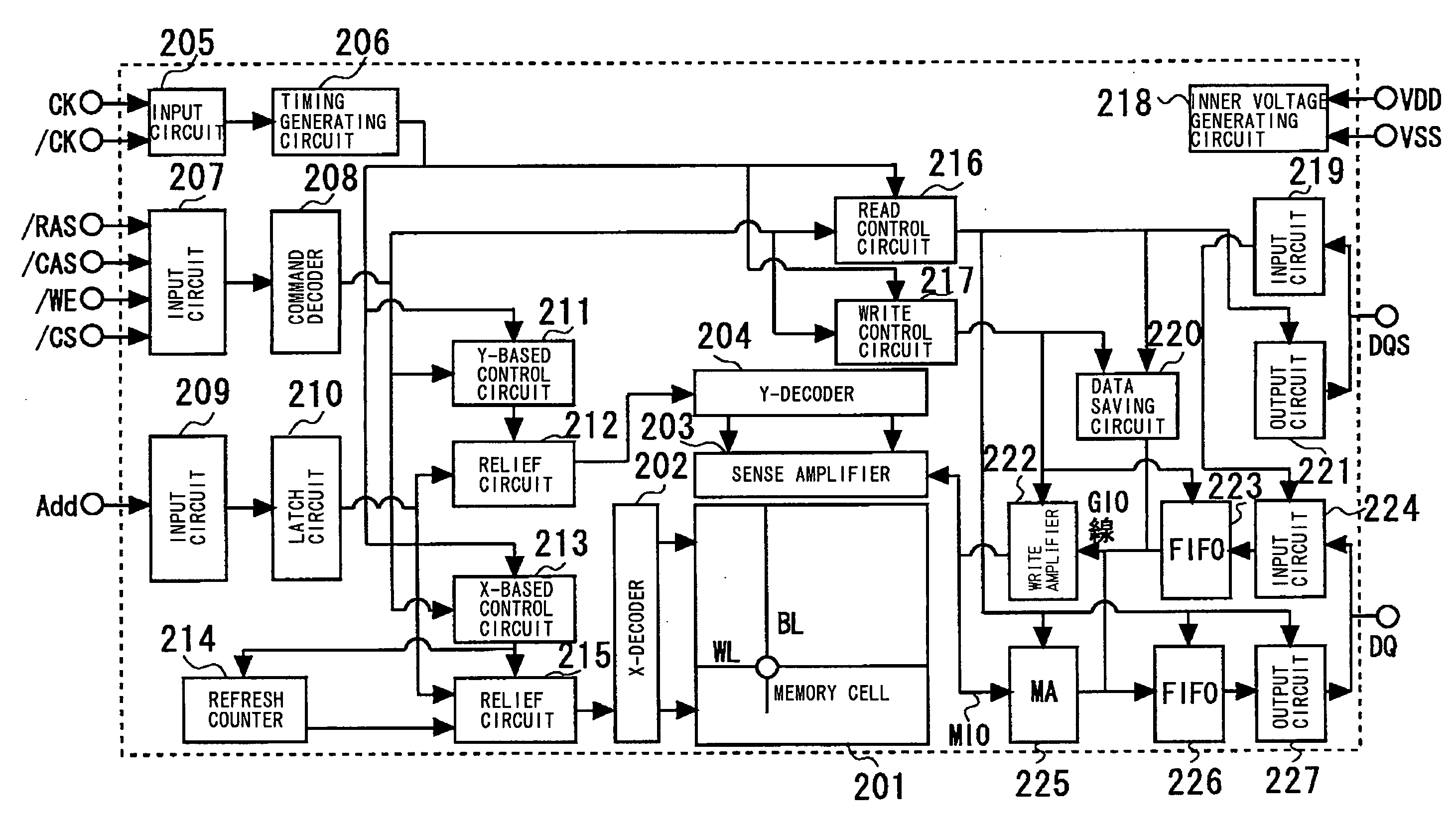
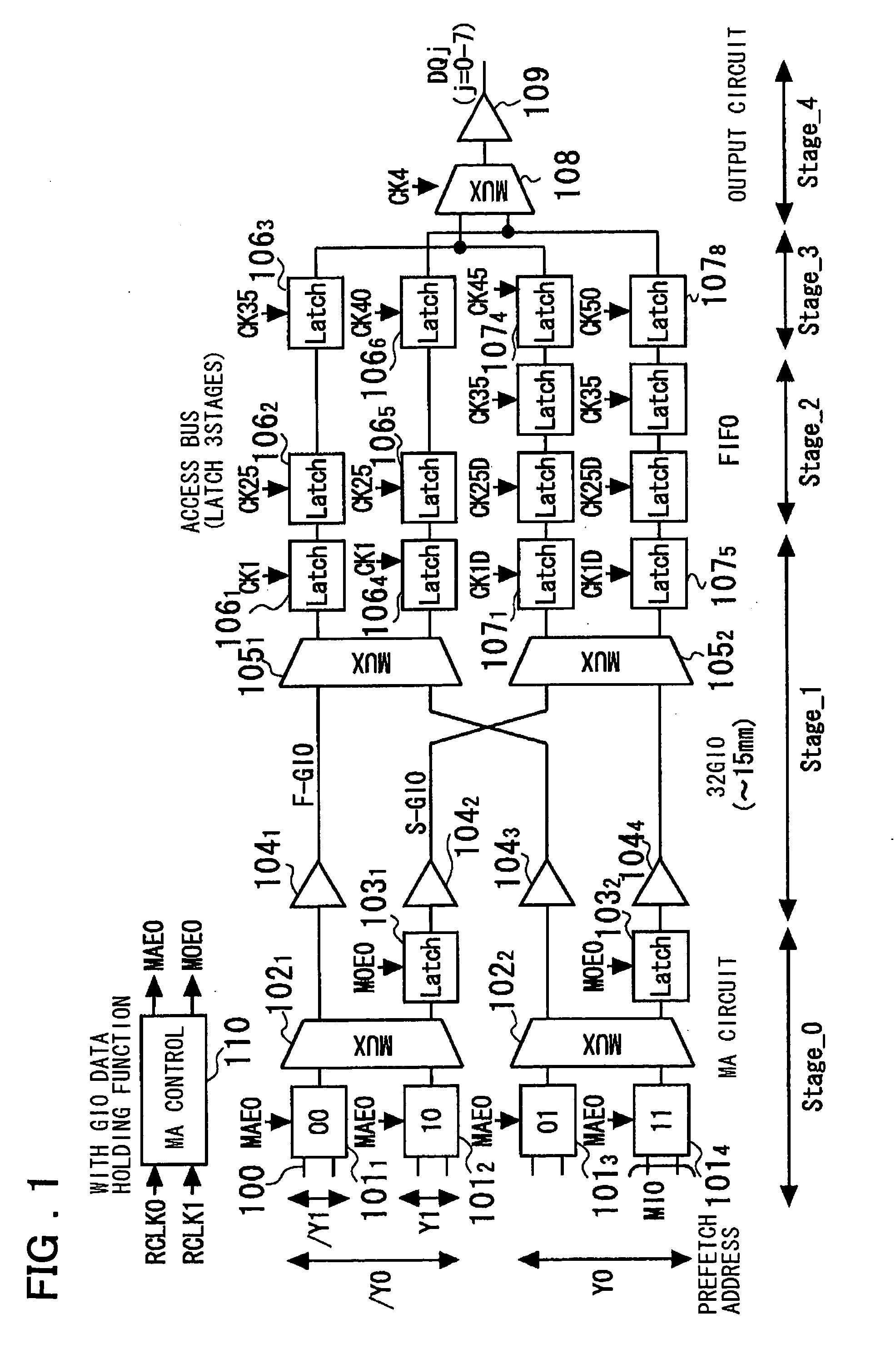
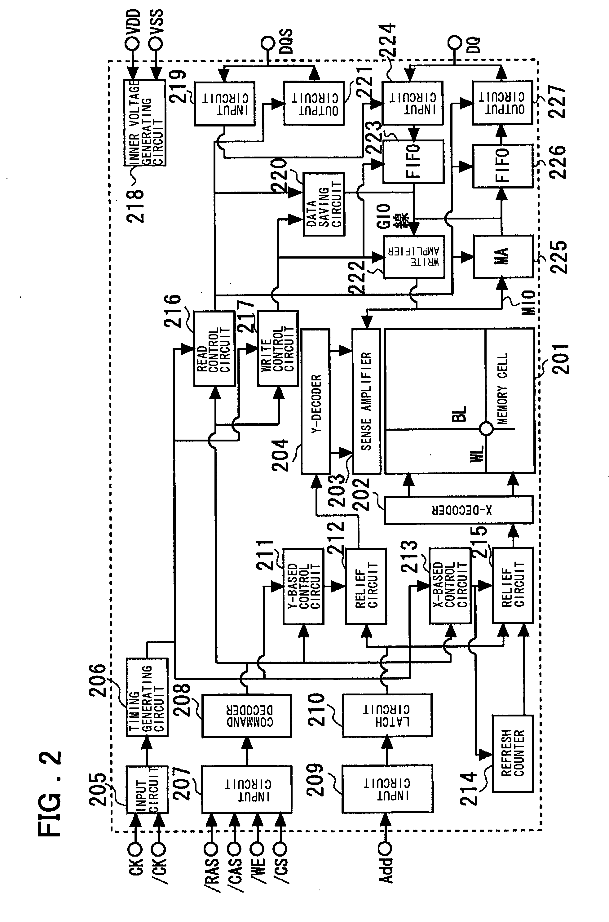
[0038]FIG. 1 shows a pre-fetch system data transfer circuit according to the present invention. The data transfer circuit according to the present embodiment includes an amplifier control circuit 110 supplied with first and second read control signals (RCKL0 and RCLK1) of respective different phases, obtained on frequency dividing by 2 of a clock signal supplied to a semiconductor storage device to generate first and second control signals (MAE0 and MOE0) of respective different phases, and first to fourth amplifiers (main amplifiers 1011 to 1014), supplied with read data from the memory cell array corresponding to four addresses from a main input / output line (MIO) and with the common control signal (MAE0) in common to amplify and output read data corresponding to the four addresses responsive to the fi...


PUM


Abstract

A semiconductor storage device has a data transfer circuit capable of reducing the latency, including a control circuit for frequency-dividing external clock signal to generate readout clocks, first to fourth amplifier circuits for amplifying read data corresponding to first and fourth addresses, based on readout clock signals, a first multiplexer receiving and selectively outputting temporally preceding and temporally succeeding first and second output data from two amplifier circuits associated with two even addresses, a second multiplexer receiving and selectively outputting temporally preceding and temporally succeeding third and fourth output data from two amplifier circuits associated with two odd addresses, first and second latch circuits for latching and outputting second and fourth output data, a third multiplexer receiving first and third data and outputting the latched data in the read address sequence, a fourth multiplexer receiving second and fourth data and outputting the latched data in the read address sequence, first and second registers receiving outputs of the third and fourth multiplexers, and a fifth multiplexer sending out two outputs each of the first and second registers, totaling at four outputs, in synchronism with rising and falling edges of the clock signal.

Description

FIELD OF THE INVENTION [0001] This invention relates to a semiconductor integrated circuit device and, more particularly, to a data transfer circuit having a pre-fetch memory for simultaneously reading out plural bits from memory cells and for serially outputting the so read-out bits. BACKGROUND OF THE INVENTION [0002] The pre-fetch memory data transfer system of this sort is generally meritorious in improving the operating frequency in a clock synchronized semiconductor storage device. In actuality, in a DDR (Double Data Rate)-1 SDRAM (Synchronous Dynamic Random Access Memory), and in a DDR-2 SDRAM, the data transfer rate is improved by increasing the number of pre-fetch to 2N and to 4N (N=1; number of I / Os per address), respectively. However, the access time speedup of the chip itself cannot be achieved with ease. [0003] Hence, only the data transmitting rate is improved, without improving the access time, by increasing the latency with increase in the operating frequency. [0004] ...

Claims


Application Information

Patent Timeline
IPC IPC(8): G11C11/409G11C5/00G11C7/10G11C7/22G11C11/401G11C11/407G11C11/4076G11C11/4096H01L21/8242H01L27/108
CPCG11C7/1012G11C7/1039G11C7/1066G11C2207/107G11C7/222G11C11/4076G11C11/4096G11C7/22
Inventor FUJISAWA, HIROKI
Owner LONGITUDE LICENSING LTD
Why Eureka
Try Eureka