

Semiconductor device and manufacturing method
a technology of semiconductor devices and manufacturing methods, applied in the direction of semiconductor devices, electrical devices, transistors, etc., can solve the problems of increasing the cost of the production process of semiconductor devices such as lsi, difficulty in further refinement of fabrication, and the method described above has not yet been put to practical use, and achieves excellent drain current characteristics
- Summary
- Abstract
- Description
- Claims
- Application Information
AI Technical Summary
Benefits of technology
Problems solved by technology
Method used
Image

Examples
Embodiment Construction
[0048] Preferred embodiments of the present invention are to be described below. The invention is not restricted to the following embodiments but is applicable to other embodiments.
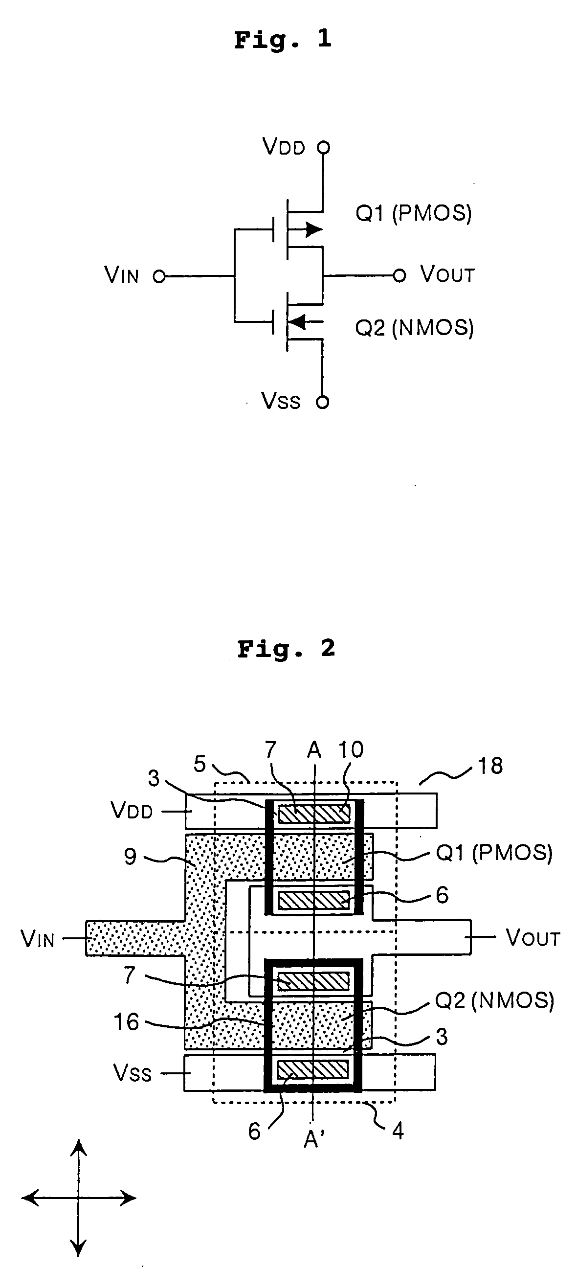
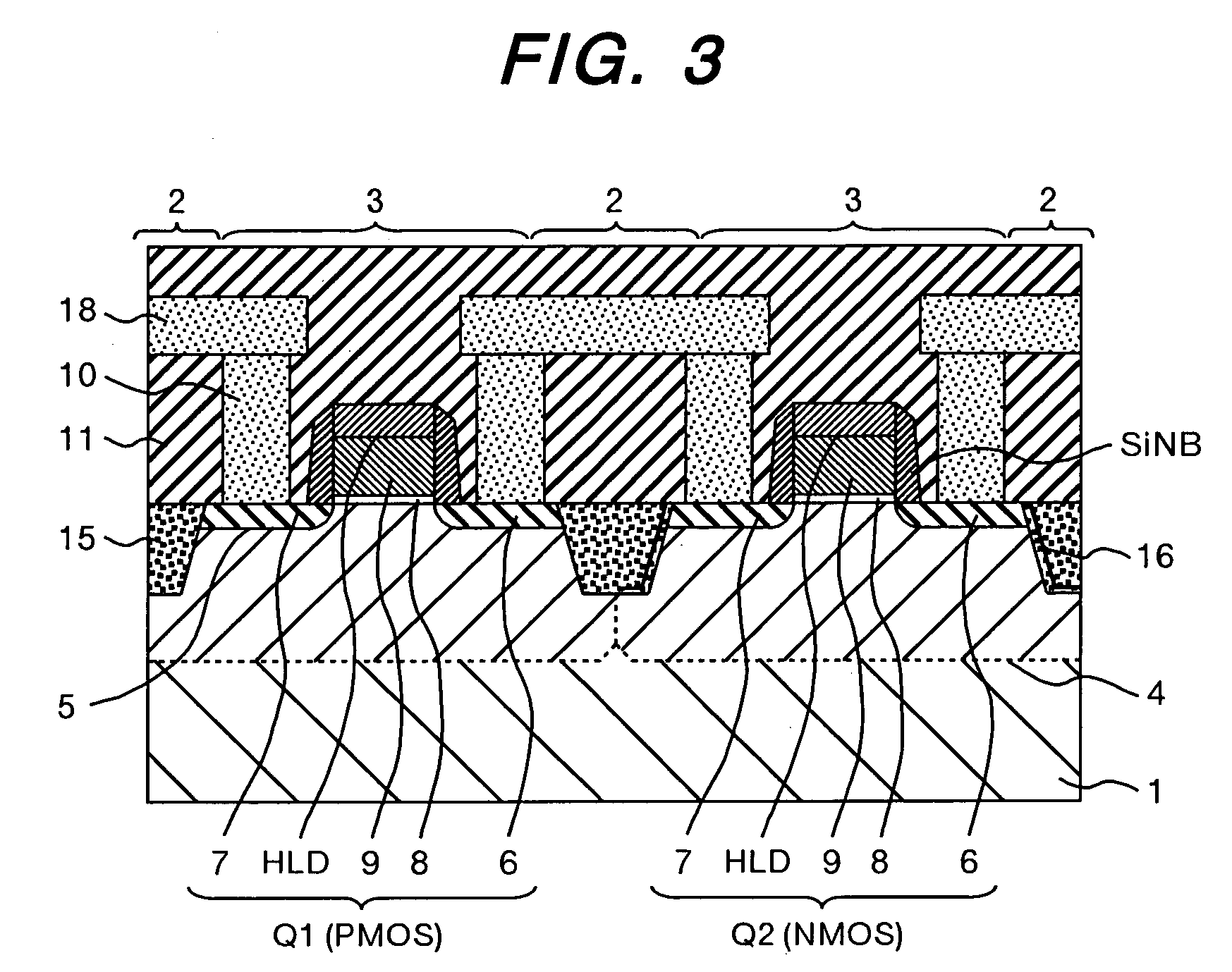
[0049] The invention is to be described by way of the first embodiment with reference to FIG. 1. FIG. 1 is an inverter circuit diagram of this embodiment; FIG. 2 is a layout of the inverter circuit; and FIG. 3 is a cross-sectional view taken along line A-A′ of FIG. 2.
[0050] As shown in FIG. 2, this embodiment comprises a p-type channel field effect transistor Q1, an n-type channel field effect transistor Q2 and interconnections for connecting the transistors electrically.
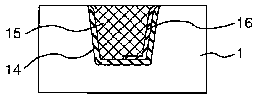
[0051] The n-type channel field effect transistor Q2 formed on a substrate (sub1) 1 comprises an n-type source (soce 1) 6, a drain (drain 1) 7, a gate electrode (poly-Si) 9 and a gate oxide film (gato-ox) 8 formed on a p-type well layer (pwell) 4. Further, the p-type channel field effect transistor Q1 comprises a p-type source (soce) 6...
PUM
 Abstract
Description
Claims
Application Information