Thin film magnetic memory device including memory cells having a magnetic tunnel junction

a magnetic memory, thin film technology, applied in semiconductor devices, digital storage, instruments, etc., can solve the problems of degrading the operation reliability of the mram device, mtj memory cells having such characteristics are extremely susceptible to magnetic noise, and the data read speed cannot be increased, so as to reduce the amount of data write current, and improve the operation reliability

Inactive Publication Date: 2005-06-16
RENESAS TECH CORP
View PDF22 Cites 11 Cited by
  • Summary
  • Abstract
  • Description
  • Claims
  • Application Information

AI Technical Summary

Benefits of technology

[0058] Therefore, a primary advantage of the present invention is that the data read speed can be increased by rapidly producing a voltage change on the first bit line by conducting the data read operation with a reduced RC constant of the data read current path, without supplying any data read current to the first read data line.
[0059] According to another aspect of the present invention, a thin film magnetic memory device having a normal operation mode and a test mode includes a memory array, a plurality of write word lines, a write word line driver, a data write circuit, and a plurality of bit line pairs. The memory array includes a plurality of magnetic memory cells arranged in rows and columns. Each of the plurality of magnetic memory cells has a different resistance value according to a level of storage data written when a data write magnetic field applied by first and second data write currents is larger than a predetermined magnetic field. The plurality of write word lines are provided corresponding to the respective rows of the magnetic memory cells, and selectively activated according a row selection result in a data write operation. The write word line driver supplies the first data write current to the activated word line in an amount corresponding to a voltage level on a first control node. The data write circuit supplies the second data write current in the data write operation in an amount corresponding to a voltage level on a second control node. The plurality of bit lines are provided corresponding to the respective columns of the magnetic memory cells, and selectively connected to the data write circuit according to a column selection result in the data write operation. At least one of the write word line driver and the data write circuit includes an input terminal for externally setting the voltage level of a corresponding one of the first and second control nodes in the test mode.
[0060] Accordingly, in the test mode, at least one of the first and second data write currents can be set from the outside. Thus, the manufacturing variation in magnetic characteristics of the MTJ memory cells can be compensated for, whereby the adjustment testing of the data write current amount for appropriately ensuring a data write margin can be facilitated.
[0061] According to a further aspect of the present invention, a thin film magnetic memory device includes a memory array, a plurality of bit lines, a plurality of write word lines, and a coupling circuit. The memory array includes a plurality of magnetic memory cells arranged in rows and columns. Each of the plurality of magnetic memory cells includes a magnetic storage portion having a different resistance value according to a level of storage data written when a data write magnetic field applied by first and second data write currents is larger than a predetermined magnetic field. The plurality of bit lines are provided corresponding to the respective columns of the magnetic memory cells, for passing the first data write current therethrough. The plurality of write word lines are provided corresponding to the respective rows of the magnetic memory cells, and selectively activated according an address selection result so as to pass the second data write current therethrough in a data write operation. Each of the write word lines includes first and second sub write word lines respectively formed in first and second metal wiring layers with the magnetic storage portions interposed therebetween in a vertical direction on a semiconductor substrate. The coupling circuit electrically couples the first and second sub write word lines to each other. The second data write current flows as a reciprocating current through the first and second sub write word lines electrically coupled to each other by the coupling circuit.
[0062] Thus, since the data write current flows as a reciprocating current through the first and second bit lines that are electrically coupled to each other, data write magnetic fields acting in the same direction can be generated in the magnetic storage portion. This reduces the amount of data write current required to generate a data write magnetic field of the same strength. As a result, reduced power consumption of the MRAM device, improved operation reliability resulting from the reduced current density of the bit line, and also reduced magnetic field noise in the data write operation can be realized.
[0063] According to a still further aspect of the present invention, a thin film magnetic memory device includes a memory array, a plurality of read word lines, a plurality of write word lines, and a plurality of bit lines. The memory array includes a plurality of magnetic memory cells arranged in rows and columns. Each of the plurality of magnetic memory cells includes a magnetic storage portion having a different resistance value according to a level of storage data written when a data write magnetic field applied by first and second data write currents is larger than a predetermined magnetic field. The plurality of read word lines are provided corresponding to the respective rows of the magnetic memory cells, and are driven to a first voltage according to a row selection result in a data read operation. The plurality of write word lines are provided corresponding to the respective rows, and are selectively activated according an address selection result so as to pass the first data write current therethrough in a data write operation. The plurality of bit lines are provided corresponding to the respective columns of the magnetic memory cells so as to extend in such a direction that crosses the plurality of write word lines, and are each coupled to the magnetic storage portions. One of the plurality of bit lines that is selected according to an address selection result passes therethrough a data read current and the second data write current in the data read operation and the data write operation, respectively. Each of the magnetic memory cells further includes a rectifying element connected between the corresponding magnetic storage portion and the corresponding read word line.

Problems solved by technology

This voltage change cannot be quickly produced with a large RC (resistance-capacitance) time constant of the sense current path, making it impossible to increase the data read operation speed.
As a result, the MTJ memory cell having such characteristics is extremely susceptible to the magnetic noise.
Electromigration may cause disconnection or short-circuit of the wirings, thereby possibly degrading the operation reliability of the MRAM device.
Moreover, an increased data write current may possibly produce a considerable amount of magnetic noise.
As described in connection with FIGS. 87 and 88, a large number of wirings are required to write and read the data to and from the MTJ memory cell, making it difficult to reduce the area of the memory array integrating the MTJ memory cells, and thus the chip area of the MRAM device.
This causes a voltage drop on these lines.
As a result, a current may unexpectedly flow through the MTJ memory cell, causing an erroneous data write operation.
Thus, the conventional MTJ memory cell using the access diode is advantageous in terms of improved integration, but is problematic in view of the stability of the data write operation.

Method used


Image

  • Thin film magnetic memory device including memory cells having a magnetic tunnel junction
  • Thin film magnetic memory device including memory cells having a magnetic tunnel junction
  • Thin film magnetic memory device including memory cells having a magnetic tunnel junction

Examples


first embodiment

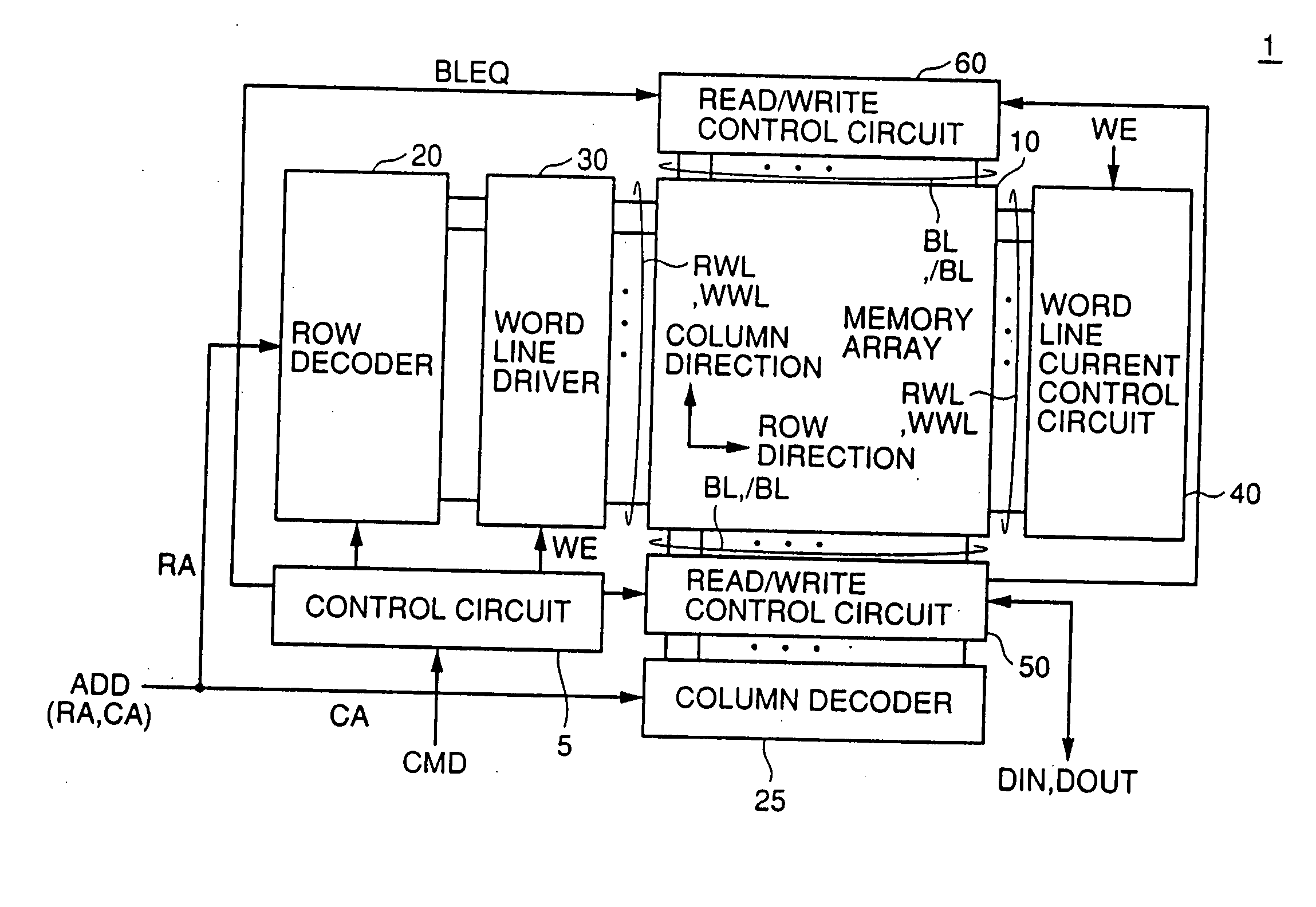
[0162] Referring to FIG. 1, an MRAM device 1 according to the first embodiment of the present invention conducts random access in response to an external control signal CMD and address signal ADD, thereby conducting input of write data DIN and output of read data DOUT.

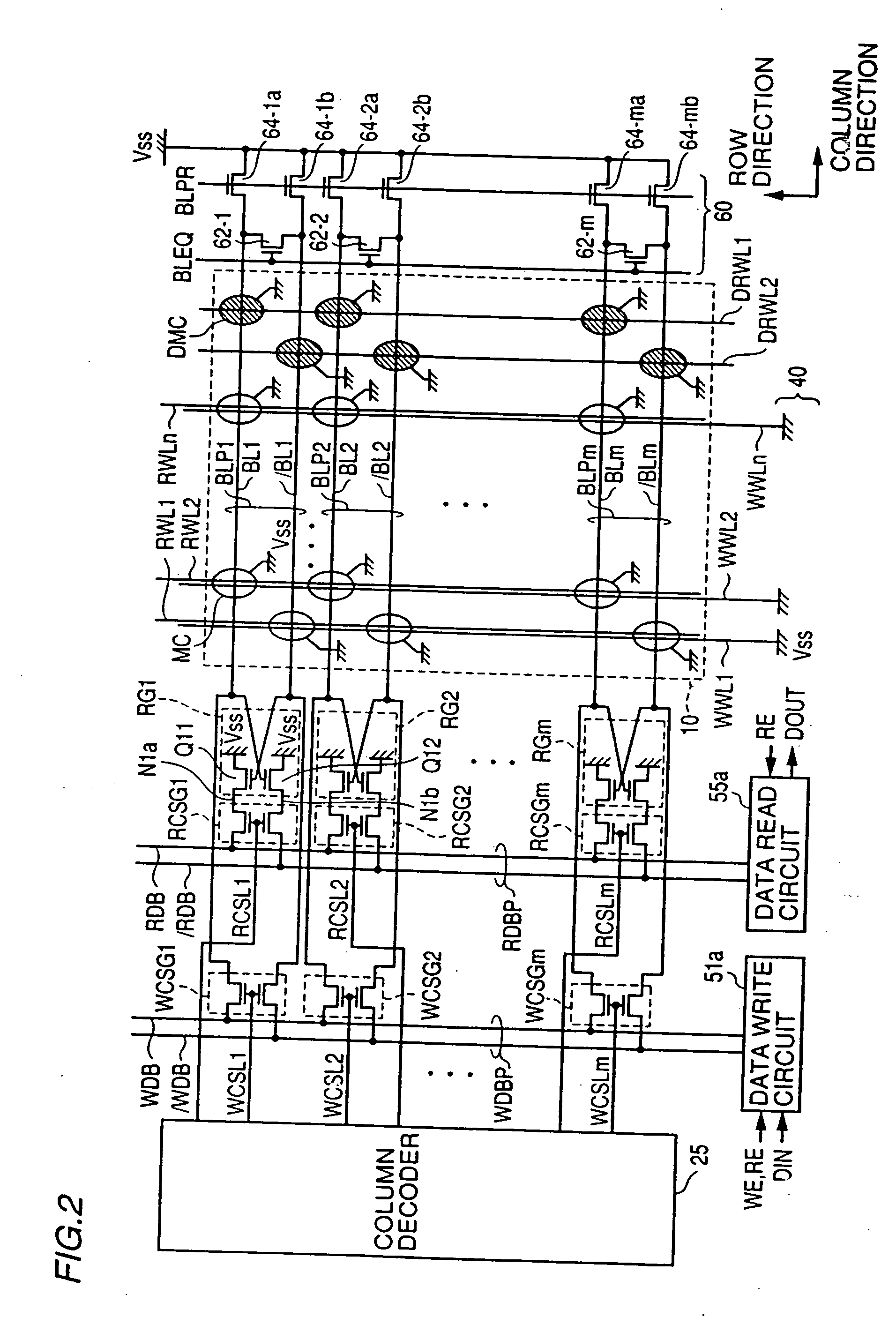
[0163] The MRAM device 1 includes a control circuit 5 for controlling the overall operation of the MRAM device 1 in response to the control signal CMD, and a memory array 10 having a plurality of MTJ memory cells arranged in n rows by m columns. Although the structure of the memory array 10 will be described later in detail, a plurality of write word lines WWL and a plurality of read word lines RWL are provided corresponding to the respective MTJ memory cell rows. Folded bit line pairs are provided corresponding to the respective MTJ memory cell columns. Each bit line pair is formed from bit lines BL and / BL. Note that, hereinafter, a set of bit lines BL and / BL is also generally referred to as a bit line pair BLP.

[0...

second embodiment

Modification of Second Embodiment

[0290] Referring to FIG. 14, a data write current adjustment circuit 230 according to the modification of the second embodiment outputs a reference voltage Vref for adjusting the amount of the data write current. Note that the data write current adjustment circuit 230 shown in FIG. 13 may be replaced either with the data write current adjustment circuit 200 for adjusting the data write current ±Iw to be supplied to the bit line or with the data write current adjustment circuit 21 for adjusting the data write current Ip to be supplied to the write word line.

[0291] Referring to FIG. 14, the data write current adjustment circuit 230 includes a tuning input portion 231a and a voltage adjustment portion 231b for adjusting the reference voltage Vref according to the setting of the tuning input portion 231a.

[0292] The voltage adjustment portion 231b includes a P-channel MOS transistor 232 electrically coupled between a node Nt1 producing the reference vol...

third embodiment

[0321] In the third embodiment is described the structure in which the bit lines BL and write word lines WWL receiving the data write current are formed in a plurality of wiring layers.

[0322]FIG. 16 shows the bit line arrangement according to the third embodiment of the present invention.

[0323] Referring to FIG. 16, the data write and read operations to and from the memory array 10 are conducted through the data I / O line pair DI / OP by the data write circuit 51b and the data read circuit 55d, respectively, based on the same structure as that of FIG. 15.

[0324] The bit lines BL1 to BLm, / BL1 to / BLm forming the bit line pairs BLP1 to BLPm, column selection gates CSG1 to CSGm, and column selection lines CSL1 to CSLm are provided corresponding to the respective memory cell columns.

[0325] The bit lines BL1 to BLm are formed in a wiling layer different from that of the bit lines / BL1 to / BLm. For example, the bit lines BL1 to BLm are each formed in a metal wiring layer M3, whereas the ...


PUM


Abstract

In the data read operation, a memory cell and a dummy memory cell are respectively coupled to two bit lines of a selected bit line pair, and a data read current is supplied thereto. In the selected memory cell column, a read gate drives the respective voltages on a read data bus pair, according to the respective voltages on the bit lines. A data read circuit amplifies the voltage difference between the read data buses so as to output read data. The use of the read gate enables the read data buses to be disconnected from a data read current path. As a result, respective voltage changes on the bit lines are rapidly produced, whereby the data read speed can be increased.

Description

BACKGROUND OF THE INVENTION [0001] 1. Field of the Invention [0002] The present invention relates to a thin film magnetic memory device. More particularly, the present invention relates to a random access memory (RAM) including memory cells having a magnetic tunnel junction (MTJ). [0003] 2. Description of the Background Art [0004] An MRAM (Magnetic Random Access Memory) device has attracted attention as a memory device capable of non-volatile data storage with low power consumption. The MRAM device is a memory device that stores data in a non-volatile manner using a plurality of thin film magnetic elements formed in a semiconductor integrated circuit and is capable of random access to each thin film magnetic element. [0005] In particular, recent announcement shows that significant progress in performance of the MRAM device is achieved by using thin film magnetic elements having a magnetic tunnel junction (MTJ) as memory cells. The MRAM device including memory cells having a magnetic...

Claims


Application Information

Patent Timeline
Patent Type & Authority Applications(United States)
IPC IPC(8): G11C11/14G11C11/15G11C11/16H01L21/8246H01L27/10H01L27/105H01L43/08
CPCG11C7/12G11C7/14G11C2207/002G11C11/16G11C11/15G11C11/1653G11C11/1655G11C11/1657G11C11/1659G11C11/1673G11C11/1675G11C11/1693
Inventor HIDAKA, HIDETO
Owner RENESAS TECH CORP
Why Eureka
Try Eureka