Methods of forming solder areas on electronic components and electronic components having solder areas

a technology of electronic components and solder areas, which is applied in the direction of conductive pattern formation, manufacturing tools, and soldering apparatus, etc., can solve the problems of affecting the physical and/or electrical properties of the contact, requiring a significant capital investment for processing equipment, and evaporation bumping generally requires a significant amount of capital investmen

Inactive Publication Date: 2005-06-23
ROHM & HAAS ELECTRONICS MATERIALS LLC
View PDF20 Cites 41 Cited by
  • Summary
  • Abstract
  • Description
  • Claims
  • Application Information

AI Technical Summary

Problems solved by technology

Of these techniques, electroplate bumping and evaporation bumping generally require a significant capital investment for the processing equipment.
A number of limitations are associated with conventional solder pastes.
Such residues may adversely affect the physical and / or electrical properties of the contact.
In order to minimize or prevent such residues, excessively high temperatures not compatible with the device or substrate materials may be required.
The bonding hierarchy thus severely limits the types of solder materials that can be used.
A further limitation to the choice of useful solder materials is the material of construction of the substrates.
For example, a switch from 70Sn / 30Pb to 70In / 30Pb results in a reduction in melting point temperature from 193° C. to 174° C. Unfortunately, these lower-melting solders often fatigue or deform (e.g., creep) during operation of electronic components, resulting in lowered reliability.
Unfortunately, the best alternatives to lead-containing materials have a higher solidus temperature relative to eutectic tin-lead.
Unfortunately, however, the solidus temperature of the Sn / Ag3.0 / Cu0.5 alloy is about 217° C., 34° C. higher than that of eutectic Sn / Pb.
There is concern that the increased thermal excursion required by this alloy may lead to premature failure of the electronic component.
The '742 patent further discloses that if the proportion of solder powder having a particle diameter of 20 μm or less is reduced, problems associated with its preparation, such as labor intensiveness, low yields and high cost, are automatically ameliorated.

Method used


Image

  • Methods of forming solder areas on electronic components and electronic components having solder areas
  • Methods of forming solder areas on electronic components and electronic components having solder areas
  • Methods of forming solder areas on electronic components and electronic components having solder areas

Examples


examples 1-10

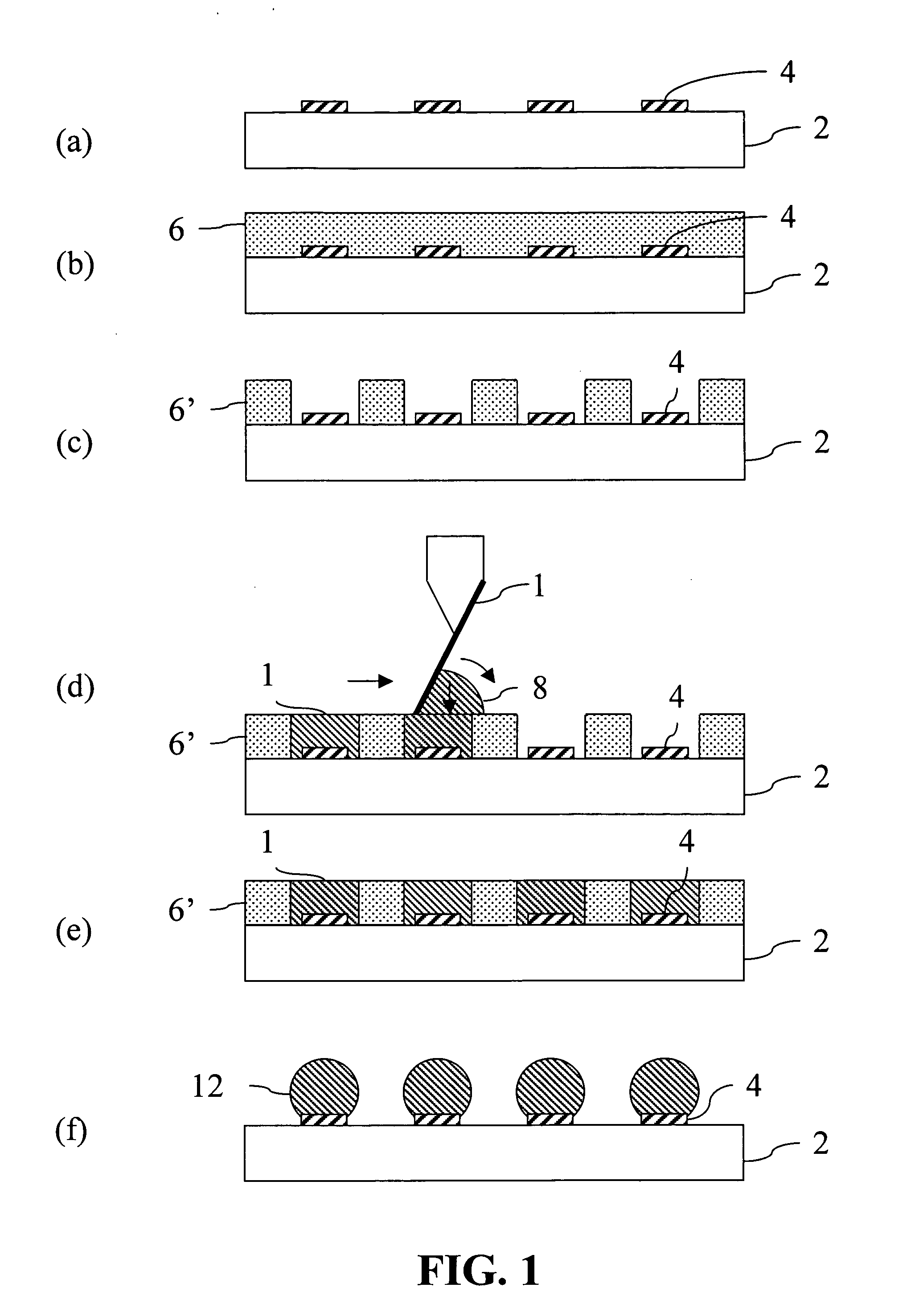
[0044] Nanoparticle solder pastes in accordance with the invention are prepared as follows. A 0.25M benzoic acid solution is prepared from 0.92 g of benzoic acid and 20 ml diethyl ether. 86 g of solder alloy nanoparticles are added to the solution and soaked for an hour with occasional stirring. The powder slurry is rinsed and dried. A rosin-based flux is prepared from 50 wt % rosin, 41 wt % glycol solvent, 4 wt % succinic acid, and 5 wt % castor oil. The flux is added to the metal particles to form a paste with 88 wt % metal by weight, as described in Table 1. The resulting solder pastes are used to form solder areas on electronic devices as described below.

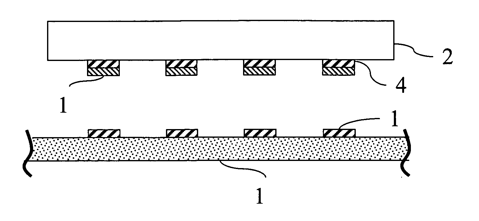
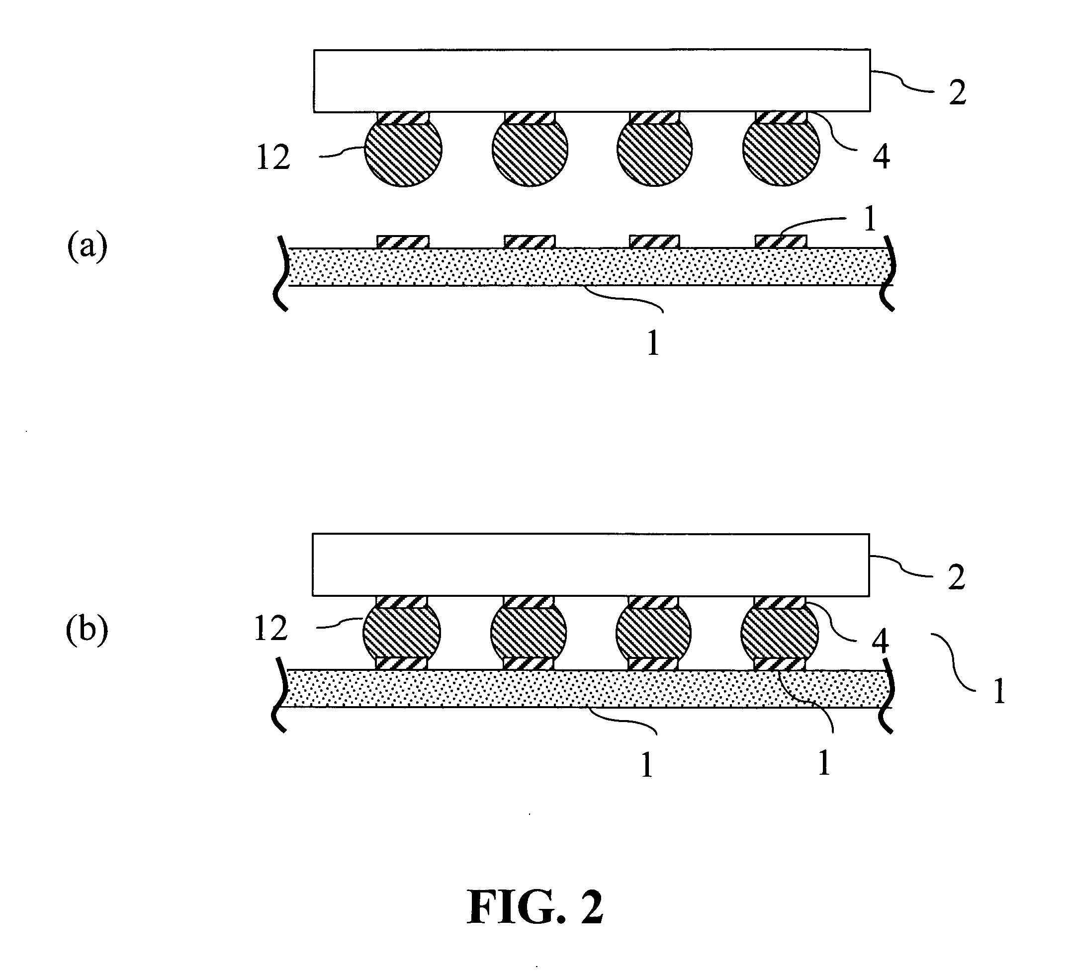
[0045] Semiconductor wafers having IC chips formed on the surface thereof are provided. Each IC chip has 64 contact pads (200 μm on each side) at a pitch of 100 μm. A metal mask is placed in contact with the surface, the mask having openings with a diameter of 150 μm exposing the contact pads . Solder paste is spread across the...


PUM

PropertyMeasurementUnit
diameteraaaaaaaaaa
diameteraaaaaaaaaa
temperatureaaaaaaaaaa

Abstract

Disclosed are methods of forming solder areas on electronic components. The methods involve: (a) providing a substrate having one or more contact pads; and (b) applying a solder paste over the contact pads. The solder paste includes a carrier vehicle and a metal component having metal particles. The solder paste has a solidus temperature lower than the solidus temperature that would result after melting of the solder paste and resolidification of the melt. Also provided are electronic components which can be formed by the inventive methods. Particular applicability can be found in the semiconductor industry in the formation of interconnect bumps on a semiconductor component, for example, for bonding an integrated circuit to a module circuit or printed wiring board using a bump bonding process.

Description

CROSS-REFERENCE TO RELATED APPLICATIONS [0001] This application claims the benefit under 35 U.S.C. § 119(e) of U.S. Provisional Application No. 60 / 532,264, filed Dec. 22, 2003, the entire contents of which are incorporated herein by reference.BACKGROUND OF THE INVENTION [0002] This invention relates to methods of forming solder areas on electronic components. As well, the invention relates to electronic components having solder areas. Particular applicability can be found in the semiconductor industry in the formation of interconnect bumps on a semiconductor device, for example, for bonding an integrated circuit (IC) to a module circuit, an interposer, or a printed wiring board (PWB) using a solder bump bonding process. [0003] There is a current focus in the semiconductor manufacturing industry on wafer-level-packaging (WLP). In wafer-level-packaging, IC interconnects are fabricated en masse on a wafer, and complete IC modules can be built on the wafer before it is diced. Benefits g...

Claims


Application Information

Patent Timeline
Patent Type & Authority Applications(United States)
IPC IPC(8): H01L21/60B23K3/06B23K31/02H05K3/00H05K3/12H05K3/34H05K13/04
CPCB23K3/0638H01L2924/014H01L24/11H01L24/81H01L2224/1147H01L2224/13099H01L2224/16H01L2224/81801H01L2924/01013H01L2924/01022H01L2924/01029H01L2924/0103H01L2924/01032H01L2924/01033H01L2924/01046H01L2924/01047H01L2924/01049H01L2924/01051H01L2924/01057H01L2924/01075H01L2924/01078H01L2924/01079H01L2924/01082H01L2924/01322H01L2924/01327H01L2924/04941H01L2924/14H05K3/3463H05K3/3484H05K2201/0257H05K2203/043H01L2924/01005H01L2924/01006H01L2924/01024H01L2924/0105H01L2924/01074B23K2201/40B23K2101/40H01L24/05H01L24/13H01L2224/05568H01L2224/05573H01L2224/05611H01L2224/05624H01L2224/05644H01L2224/05647H01L2224/05655H01L2224/05664H01L2224/05666H01L2924/12042H05K3/3485H01L2924/00H01L2924/00014H05K3/12
Inventor BRESE, NATHANIEL E.TOBEN, MICHAEL P.
Owner ROHM & HAAS ELECTRONICS MATERIALS LLC
Why Eureka
Try Eureka