Gap-fill techniques

a gap-filling and dielectric material technology, applied in the field of gap-filling techniques, can solve the problems of increasing the risk of damage to devices fabricated on the substrate, too high aspect ratio, and inability to completely fill, etc., to achieve the effect of improving the gap-filling performance of a dielectric material and plasma-enhanced chemical vapor deposition

Inactive Publication Date: 2005-06-23
APPLIED MATERIALS INC
View PDF36 Cites 102 Cited by
  • Summary
  • Abstract
  • Description
  • Claims
  • Application Information

AI Technical Summary

Benefits of technology

[0011] A variety of techniques may be employed, separately or in combination, to improve the gap-filling performance of a dielectric material formed by chemical vapor deposition (CVD). In one approach, a first dielectric layer is deposited using sub-atmospheric chemical vapor deposition (SACVD), followed by deposition of a second dielectric layer by plasma-assisted chemical vapor deposition techniques such as high density plasma chemical vapor deposition (HDP-CVD) or plasma-enhanced chemical vapor deposition (PECVD). In another approach, a dielectric layer is deposited using SACVD in the presence of reactive ionic species from a remotely generated plasma, which acts to perform etching during the deposition process. In still another approach, high aspect trenches may be filled utilizing SACVD in combination with subsequent high temperature deposition of oxide layers.

Problems solved by technology

Gaps having a combination of a high aspect ratio and a small width present a challenge for semiconductor manufacturers to completely fill.
In short, the challenge usually is to prevent the deposited film from growing in a manner that closes off the gap before it is filled
While a TEOS-based chemistry does indeed have improved gap fill capabilities, it too runs up against limitations when required to completely fill sufficiently high aspect ratio, small-width gaps
As integrated circuit feature sizes some of the devices fabricated on the substrate become increasingly sensitive to damage that may be caused by plasma processing techniques including the dep / etch / dep and HDP-CVD techniques described above.
In addition to depositing a desired film over the substrate, thermal CVD and plasma enhanced CVD deposition techniques typically leave unwanted deposition material on interior surfaces of the deposition chamber including the chamber walls.

Method used


Image

  • Gap-fill techniques
  • Gap-fill techniques
  • Gap-fill techniques

Examples


Embodiment Construction

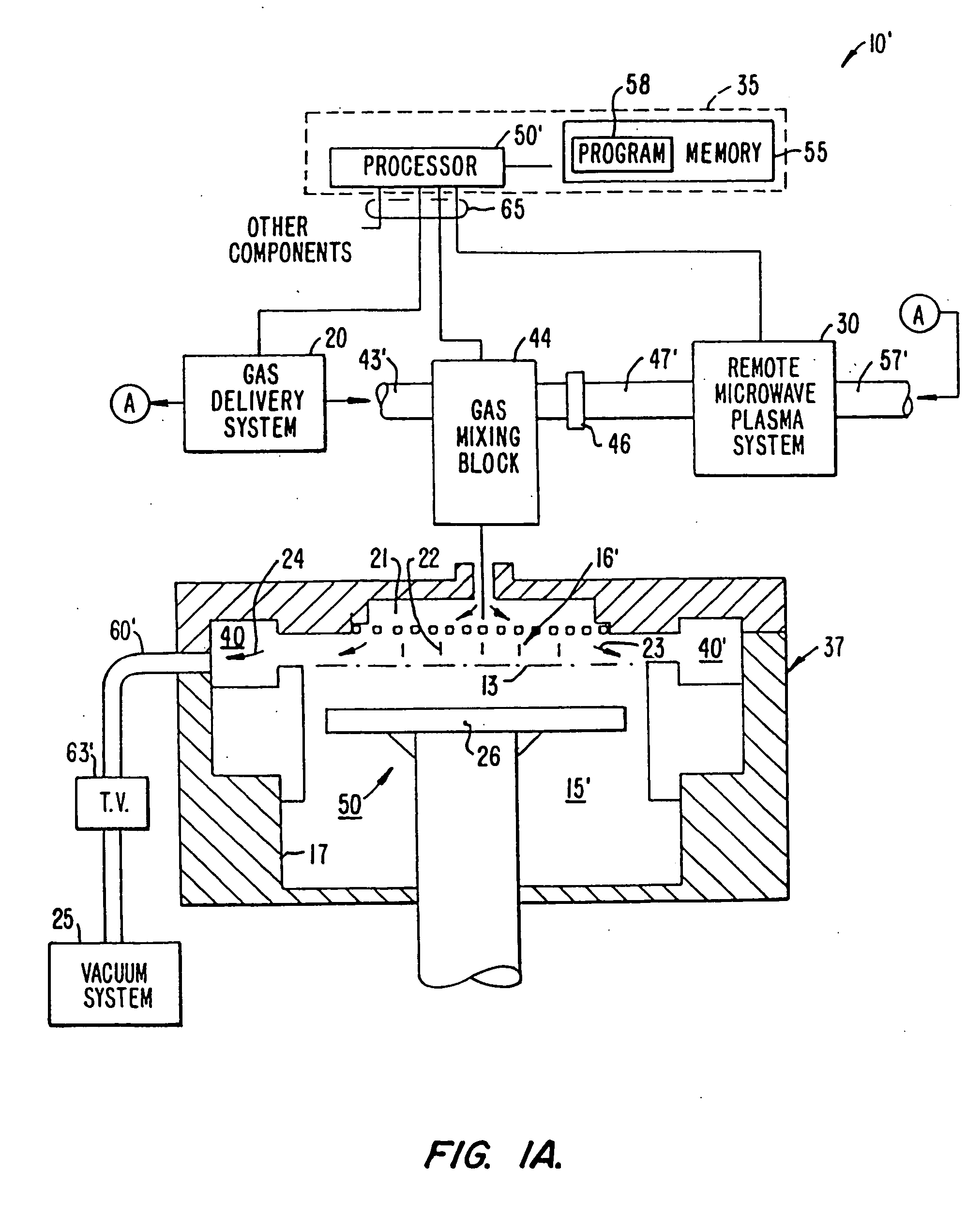
[0021] A variety of techniques may be employed, separately or in combination, to improve the gap-filling performance of a dielectric material formed by chemical vapor deposition (CVD). In one approach, a first dielectric layer is deposited using sub-atmospheric chemical vapor deposition (SACVD), followed by deposition of a second dielectric layer by plasma-assisted deposition such as HDP-CVD or PECVD. In another approach, a dielectric layer is deposited using SACVD in the presence of reactive ionic species from a remotely generated plasma, which acts to perform etching during the deposition process. In still another approach, high aspect trenches may be filled utilizing SACVD in combination with high temperature deposition of oxide layers.

I. Gap Fill Techniques

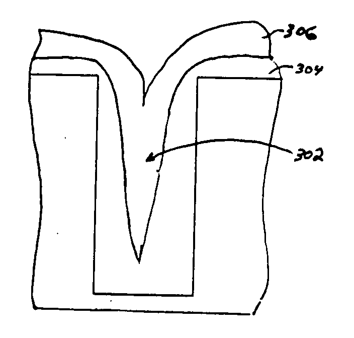
[0022] As device geometries shrink, void-free filling of high aspect ratio spaces becomes increasingly difficult due to limitations of existing deposition processes. High density plasma CVD of silicon dioxide is conventiona...


PUM

PropertyMeasurementUnit
temperatureaaaaaaaaaa
feature sizesaaaaaaaaaa
pressuresaaaaaaaaaa

Abstract

A variety of techniques may be employed, separately or in combination, to improve the gap-filling performance of a dielectric material formed by chemical vapor deposition (CVD). In one approach, a first dielectric layer is deposited using sub-atmospheric chemical vapor deposition (SACVD), followed by a second dielectric layer deposited by high density plasma chemical vapor deposition (HDP-CVD) or plasma-enhanced chemical vapor deposition (PECVD). In another approach, a SACVD dielectric layer is deposited in the presence of reactive ionic species flowed from a remote plasma chamber into the processing chamber, which performs etching during the deposition process. In still another approach, high aspect trenches may be filled utilizing SACVD in combination with oxide layers deposited at high temperatures.

Description

BACKGROUND OF THE INVENTION [0001] One of the primary steps in the fabrication of modem semiconductor devices is the formation of a thin film on a semiconductor substrate by chemical reaction of gases. Such a deposition process is referred to as chemical vapor deposition or CVD. Conventional thermal CVD processes supply reactive gases to the substrate surface where heat-induced chemical reactions take place to produce a desired film. Plasma enhanced CVD techniques, on the other hand, promote excitation and / or dissociation of the reactant gases by the application of radio frequency (RF) energy to a reaction zone near the substrate surface, thereby creating a plasma. The high reactivity of the species in the plasma reduces the energy required for a chemical reaction to take place, and thus lowers the temperature required for such CVD processes as compared to conventional thermal CVD processes [0002] CVD techniques may be used to deposit both conductive and insulative films during the ...

Claims


Application Information

Patent Timeline
Patent Type & Authority Applications(United States)
IPC IPC(8): C23C16/04C23C16/40C23C16/505H01L21/316H01L21/762H01L21/768
CPCC23C16/045C23C16/401C23C16/505H01L21/02164H01L21/022H01L21/76837H01L21/02274H01L21/31612H01L21/76224H01L21/76828H01L21/76832H01L21/02271
Inventor MUKAI, KEVIN MIKIOBRANSHAW, KIMBERLYYUAN, ZHENGXIA, XINYUNCHEN, XIAOLINLI, DONGQINGKARIM, M. ZIAULTON, VANCHING, CARYGHANAYEIM, STEVEINGLE, NITIN K.
Owner APPLIED MATERIALS INC
Why Eureka
Try Eureka