Method for the oxidative treatment of components comprised of or containing elementary silicon and/or substantially inorganic silicon compounds
a technology of elementary silicon and substantially inorganic silicon, which is applied in the direction of electrolysis process, water/sludge/sewage treatment, lavatory sanitory, etc., can solve the problems of high operational cost (for purchase and disposal), minimum solubility of ozone, and ozone must be removed
- Summary
- Abstract
- Description
- Claims
- Application Information
AI Technical Summary
Benefits of technology
Problems solved by technology
Method used
Image
Examples
example 1
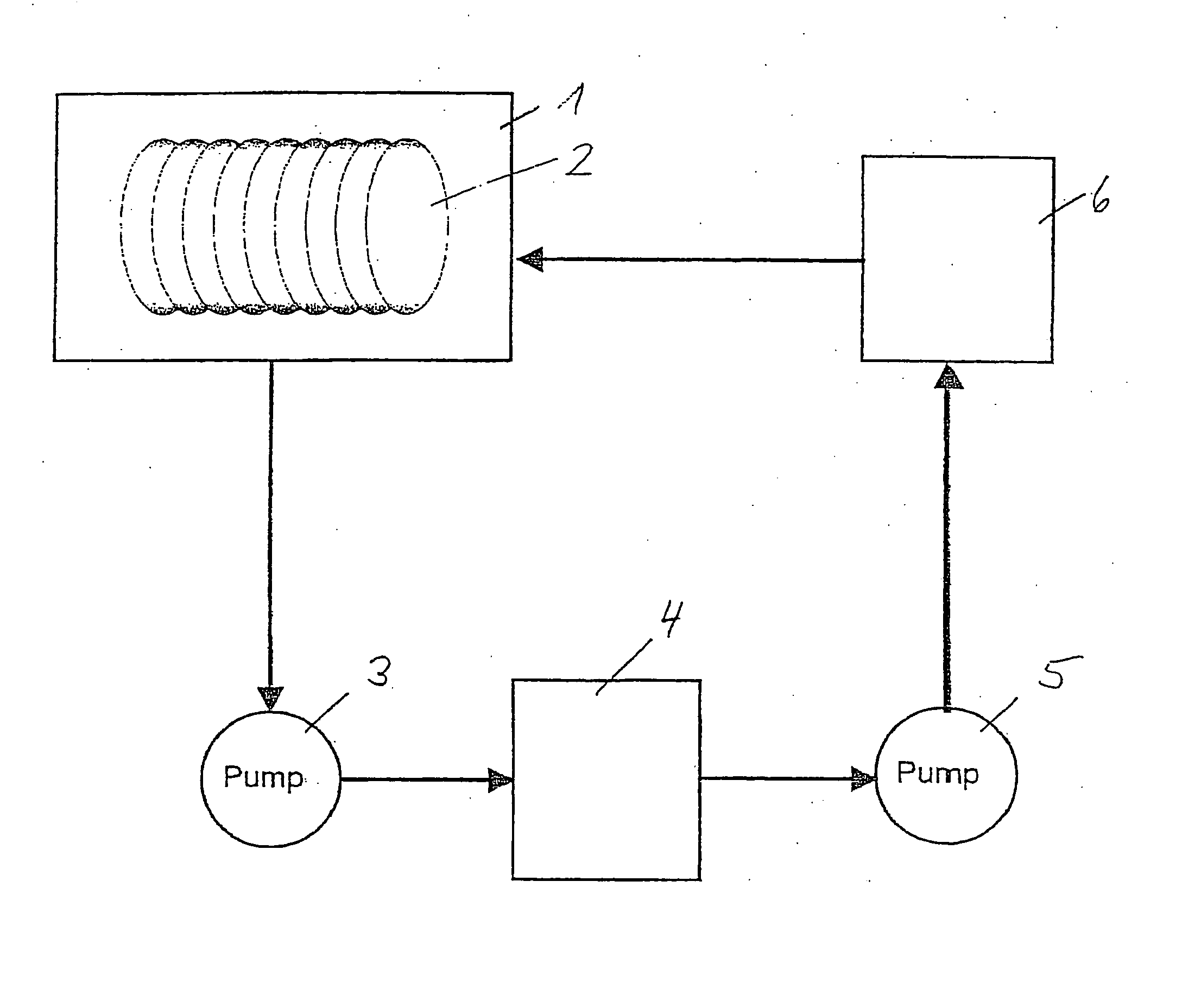
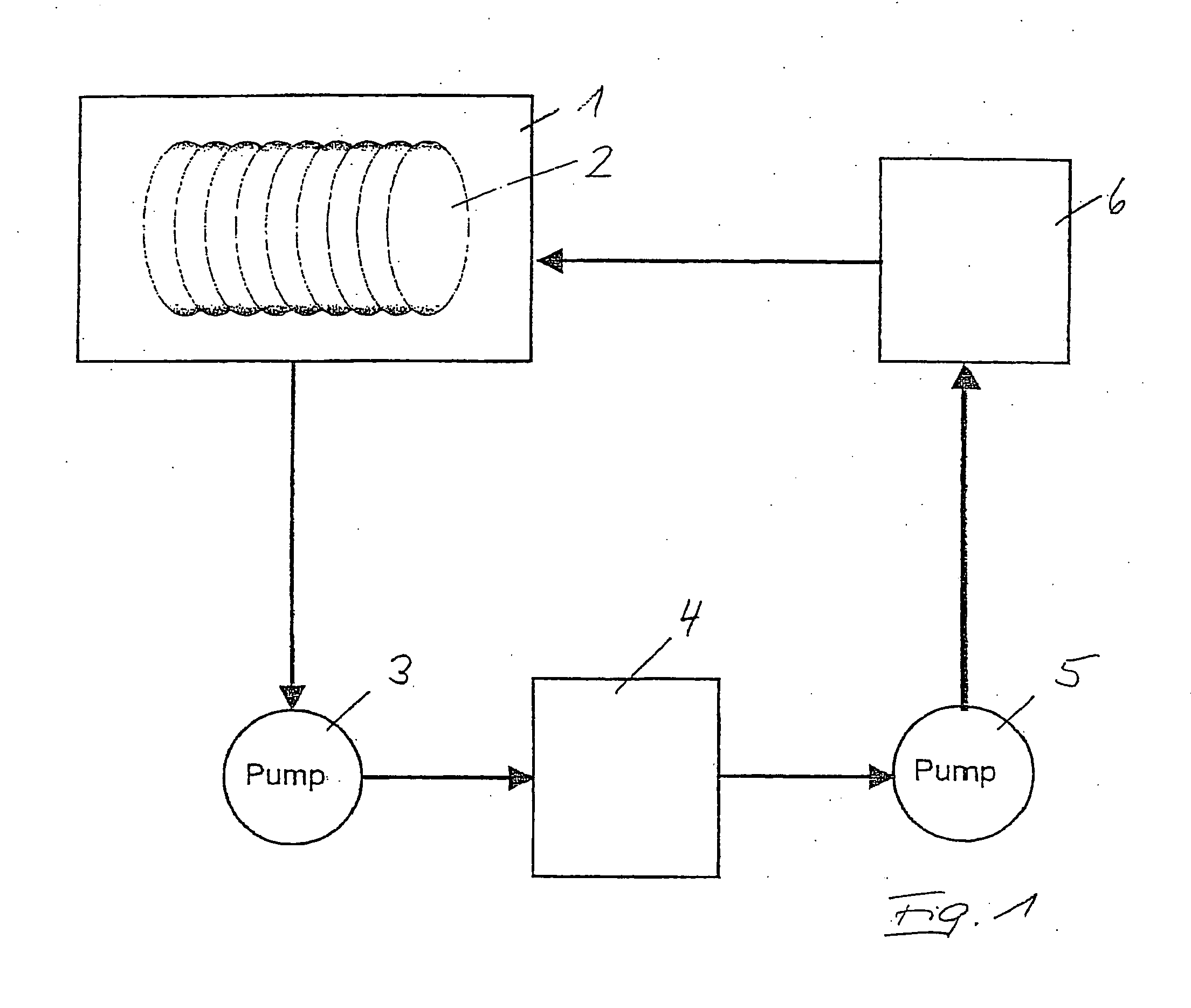
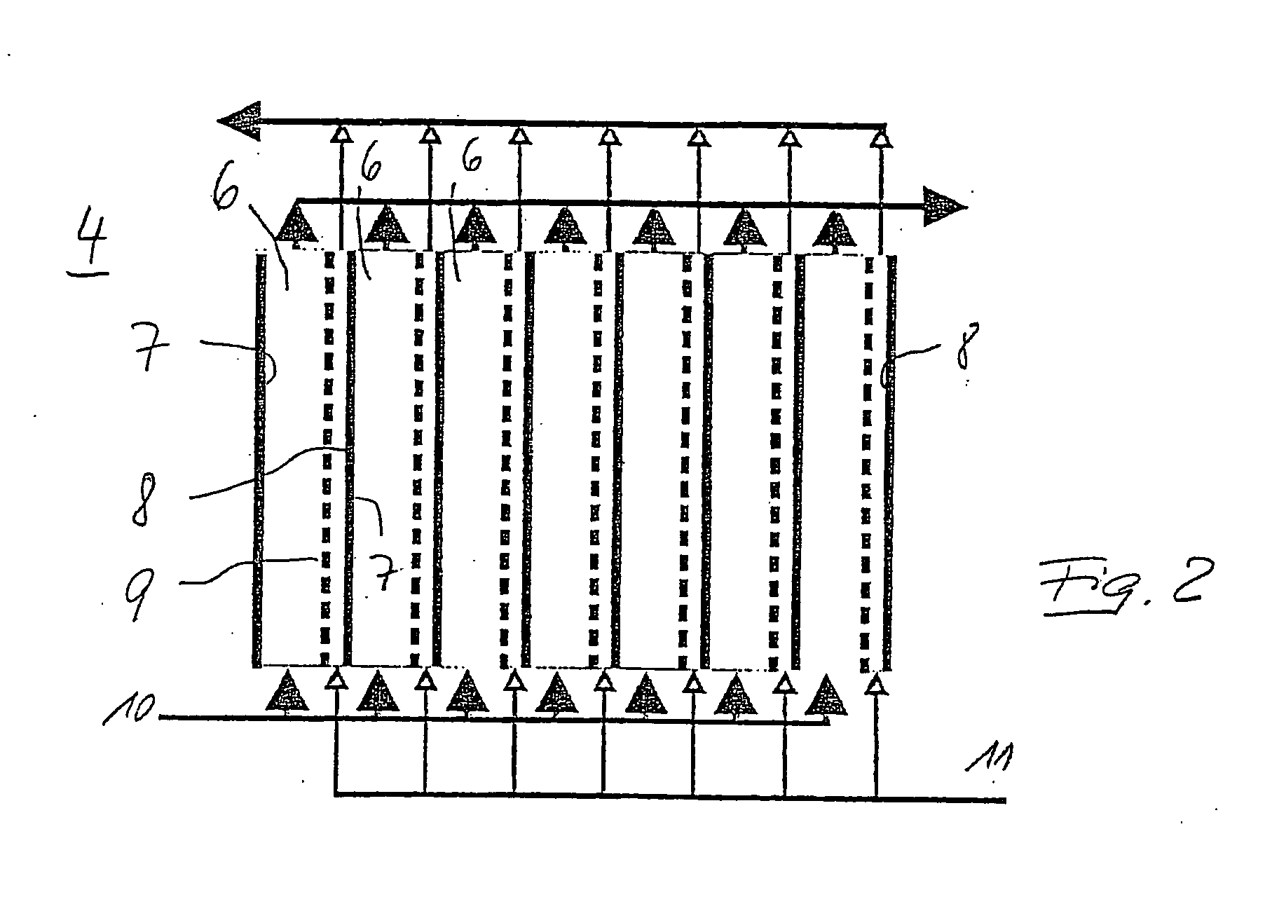
[0057] Two electrodes coated with conductive diamond were immersed in sulfuric acid of a concentration of approximately 33% in a beaker. The base of the electrodes was comprised of p-conductive silicon doped with boron and having a conductivity that corresponds to a resistivity of 5 mΩcm wherein the silicon was coated with a diamond film of a thickness of approximately 10 μm, done by means of so-called hot filament CVD. The diamond film was doped also with boron and accordingly was also p-conductive. The electrodes were contacted at the rear. The cathode was separated by a conductive membrane (Nafion® membrane) from the anode in order to prevent decomposition of the freshly formed peroxo disulfates at the cathodeode. The electrode surface was 160 cm2, the supplied current 16 A, i.e., the working current density was 100 mA / cm2. After an enrichment period of 20 hours, corresponding to approximately 11 Faraday, the solution was colored deeply yellow and heated to an equilibrium tempera...
example 2
[0058] Silicon wafers were coated with conventional photo resist (resin based on novolak, i.e., on the basis of phenols forming chains by means of CH2 groups, with diazonaphtho quinone as a photo active component that still contained residual amounts of the solvent propylene glycol monomethyl ether (PGME)). A portion of the coated wafers was subjected to conventional processes as they may be required for manufacturing microchips. One wafer was exposed to a plasma etching process. The photo resist of another wafer was irradiated with deep UV. Third and fourth wafers were exposed to ion implantation of arsenic and boron, respectively, at high doses in the range of 8×10¹⁵ / cm2 and ion energies in the range of 40-80 keV. All of these processes lead to the resist being damaged. The ion implantation moreover leads to a new crosslinking of the resist which causes incrustation of the resist surface (carbonizing). Moreover, exposed silicon dioxide is removed by sputtering, is deposited on the...
example 3
[0062] In order to simulate a spin etching process, wherein new solution is dripped continuously onto a wafer that rotates not very quickly and is spun off by centrifugal force, 0.25 ml of the oxidizing solution, prepared according to Example 1, was applied at intervals of one minute at a temperature of 50° C. onto the resist-coated wafer that had been subjected to As implantation in accordance with the parameters described in Example 2 and was positioned on a heating plate at a temperature of approximately 100-150° C. After six minutes, the wetted portion of the wafer was free of resist.
PUM
| Property | Measurement | Unit |
|---|---|---|
| temperature | aaaaa | aaaaa |
| temperature | aaaaa | aaaaa |
| temperature | aaaaa | aaaaa |
Abstract
Description
Claims
Application Information


