Single reactor, multi-pressure chemical vapor deposition for semiconductor devices

Inactive Publication Date: 2005-07-07
IBM CORP (BURLINGTON)
View PDF8 Cites 2 Cited by
  • Summary
  • Abstract
  • Description
  • Claims
  • Application Information

AI Technical Summary

Benefits of technology

[0007] The present invention provides a means to combine elements of the UHV-CVD and LPCVD processes to improve the productivity of a UHV-CVD system. In accordance with the present invention, an apparatus and a method are described for forming the semiconductor portion of CMOS, MODFET's, MOSFET's, MEMT's, NPN's and the like, along with any desired gate structure such as an ultra thin gate oxide and / or with a heavily doped polysilicon gate electrode layer to be subsequently patterned. The apparatus is an Advanced Integrated Chemical Vapor Deposition (AICVD) System having a single reaction chamber that may be operated as part of an Ultra High Vacuum-Chemical Vapor Deposition (UHV-CVD) System, a Low Pressure Chemical Vapor (LPCVD) Deposition System, and a vacuum transfer system for loading wafers from the external ambient. The vacuum transfer system includes a load-lock section for the transfer of wafers from the external ambient to an evacuated section that may remain at vacuum pressures. The evacuated section includes a single tube reactor operated as a Low Pressure / Ultra High Vacuum (LP / UHV) evacuation chamber.
[0008] The invention further comprises a low mass, rapid heating furnace in combination with three pumping packages. The three pumping packages are preferably (1) a roots blower backed by mechanical pump, (2) a turbomolecular pump backed by a roots blower and a mechanical pump, and (3) a cryopump backed by a scroll pump. By having three pumping packages communicating with the same reactor tube, each pumping package with the ability to be isolated from the reactor with a corresponding gate valve, operation of the apparatus may be rapidly transitioned from an LP vacuum (100 to 500 mtorr) process to an ultra high vacuum (0.1 to 1.0 mtorr) process. Since the wafers being treated are maintained under a vacuum in the same reactor environment, the transition between depositing sequential film layers may be seamless and defect free, while providing maximum productivity.
[0009] The apparatus and method of the invention also provides precise control of transitions from the LPCVD process to the UHV-CVD process to prevent formation of deleterious defects. For this purpose, isolation valves are provided to isolate the roots blowers and mechanical pumps from the reaction chamber until the appropriate pressure has been attained in that chamber. An improvement in this transition is then realized by drawing a vacuum on the chamber with a cryopump to remove any residual water moisture or dopant related contaminants prior to completing the transition to a UHV-CVD process from a LPCVD process. Because of this, there is no need for process steps to “passivate” the Si surface with H2. Instead, the invention maintains an atomically clean surface during transitions between the LPCVD process and the UHV-CVD process by means of reducing the oxidizing agents to insignificant levels using a cryopump.
[0010] The cryopump provides particular benefits during the transition from LPCVD to UHV-CVD processes. Although it is possible to transition from LPCVD to UHV-CVD without the cryopump, the environment would be contaminated with residual species from the LPCVD process which are not efficiently removed by a turbomolecular pump The cryopump is proficient at removing H2O, O2, B, As, P, and other species that otherwise could accumulate on the Si surface, react with the Si surface or otherwise degrade the quality or prevent formation of the subsequent epitaxial film. Of particular importance is the transition from moderate epitaxy temperatures (approximately 700° C.) to low epitaxy temperatures (about 650° C. or lower) where, if sufficient partial pressures of O2 and H2O exist, oxides of Si can readily form on the Si surface of the wafer. A cryopump is best suited for this application due to the low volume gas load and the broad range of effectively pumped gases.
[0018] The invention thereby introduces a flexible apparatus and method capable of migrating seamlessly between LPCVD processes and UHV-CVD processes within the same reactor. The invention further introduces a method and apparatus whereby cross contaminants, such as H2O, O2, and the like, and “memory effect” contaminants, such as BPA's, and the like, can be virtually eliminated by including usage of a cryopump to mediate a process transition between coupled UHV-CVD and LPCVD processes.

Problems solved by technology

Although it is possible to transition from LPCVD to UHV-CVD without the cryopump, the environment would be contaminated with residual species from the LPCVD process which are not efficiently removed by a turbomolecular pump The cryopump is proficient at removing H2O, O2, B, As, P, and other species that otherwise could accumulate on the Si surface, react with the Si surface or otherwise degrade the quality or prevent formation of the subsequent epitaxial film.

Method used


Image

  • Single reactor, multi-pressure chemical vapor deposition for semiconductor devices
  • Single reactor, multi-pressure chemical vapor deposition for semiconductor devices
  • Single reactor, multi-pressure chemical vapor deposition for semiconductor devices

Examples


example 1

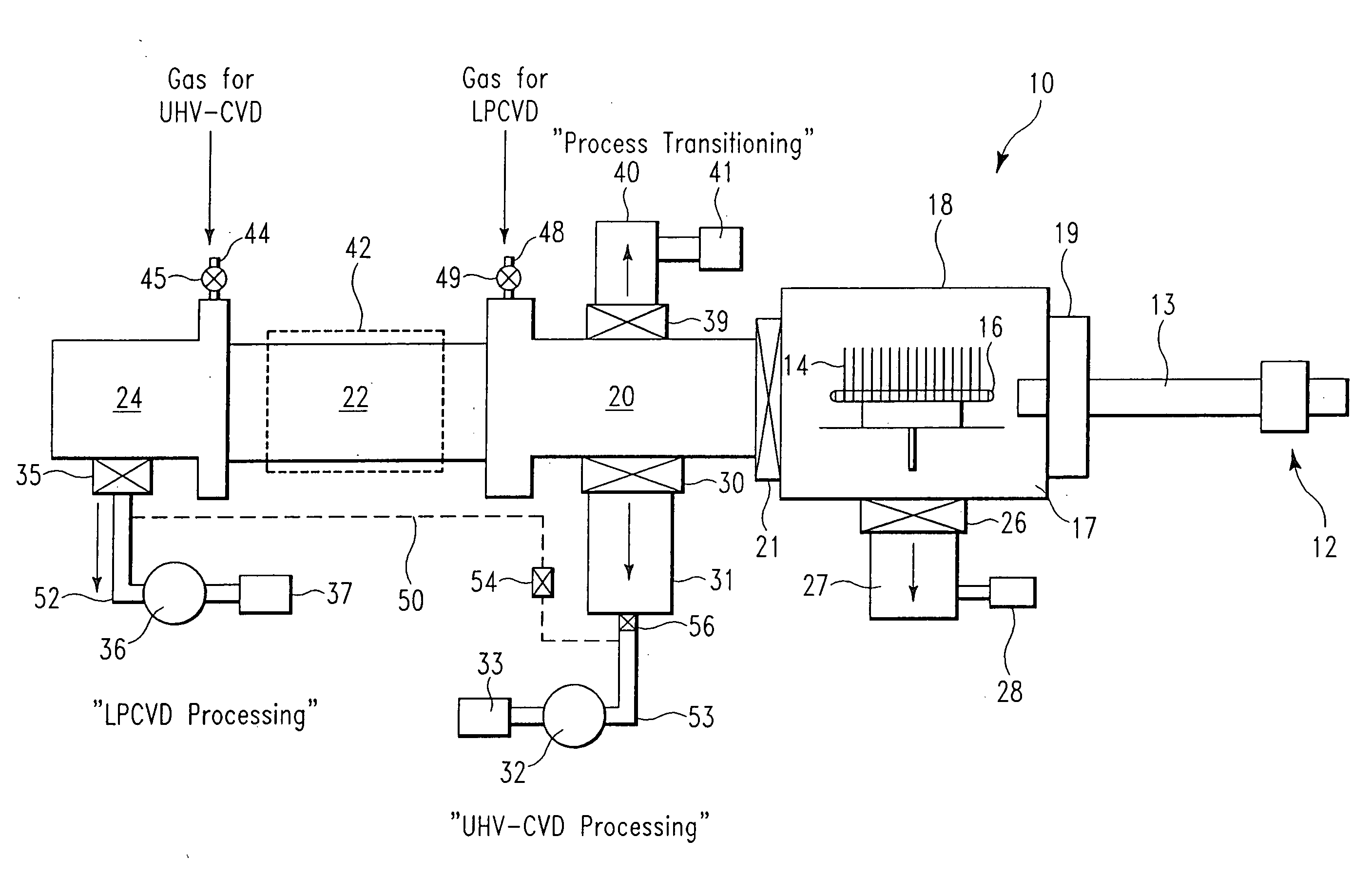
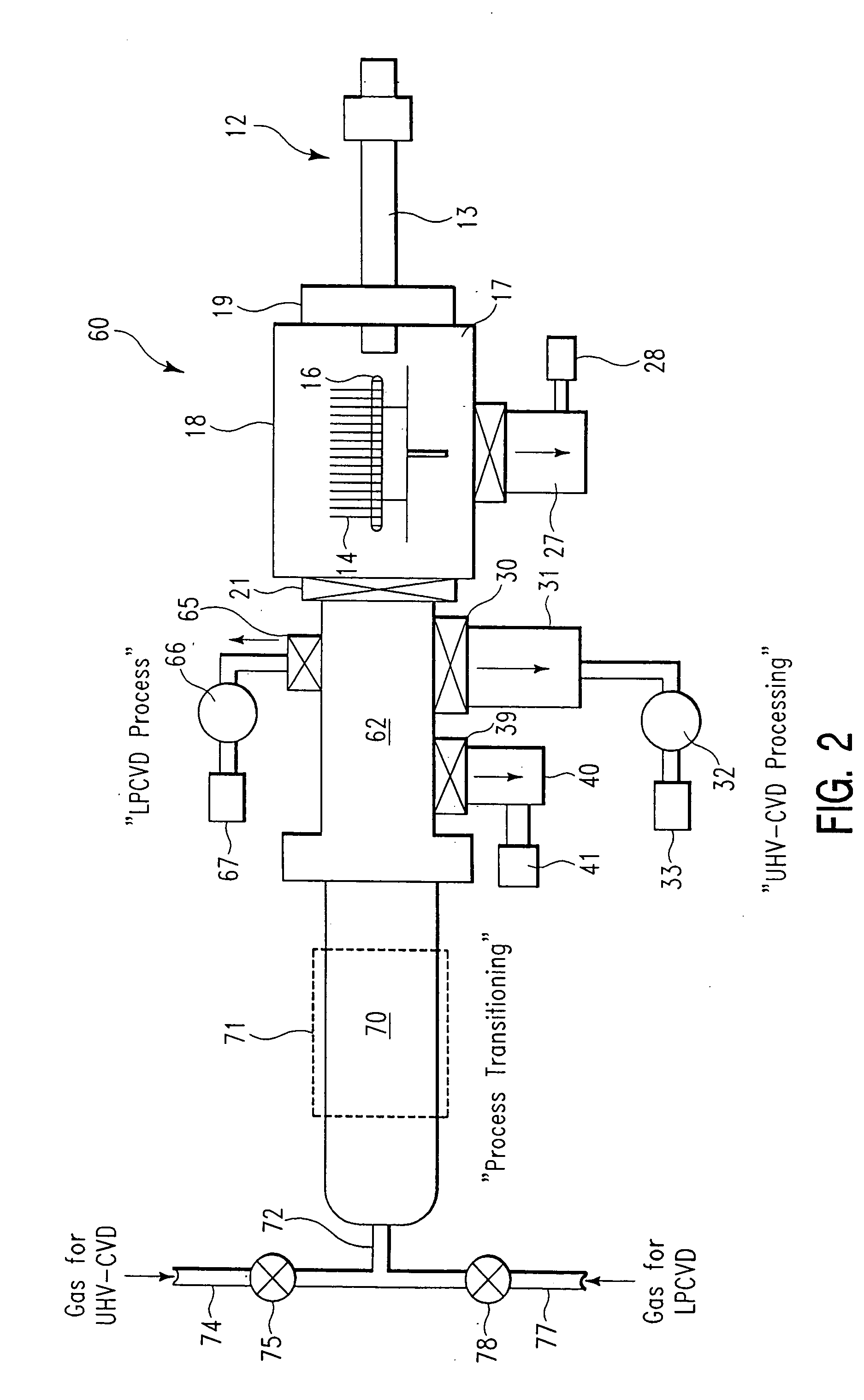
[0036] A method of operation for the AICVD system 60 shown in FIG. 2 would provide the following processes to fabricate any high performance Si and / or SiGe device structure, such as shown in FIG. 3.

[0037] Start with wafers 14 having a Si substrate 83 outside of the AICVD 60 after cleaning the wafers using a standard Huang or RCA cleaning process well known in the art.

[0038] Load the cleaned wafers 14, which may be supported on the boat 16, into the load lock chamber 18, and then transfer the wafers on boat 16 into the quartz tube reactor 70 after opening gate valve 21 and operating roots blower 66 and mechanical pump 67 to provide an LPCVD pressure environment.

[0039] Under a blanket of H2, pre-bake wafers 14 in the temperature range from 800° C. to 950° C. for 5 to 30 minutes at a process pressure of 100-500 mtorr to remove native oxides and prepare silicon surface 84.

[0040] Activate the Dichlorosilane (DCS) source, cease H2 flow, and grow the Si epitaxial pre-layer 85 to a desi...


PUM

PropertyMeasurementUnit
thicknessaaaaaaaaaa
temperaturesaaaaaaaaaa
temperatureaaaaaaaaaa

Abstract

An apparatus and method for forming at least a portion of an electronic device include a High Vacuum-Chemical Vapor Deposition (UHV-CVD) system and a Low Pressure-Chemical Vapor Deposition (LPCVD) system using a common reactor. The invention overcomes the problem, of silicon containing wafers being dipped in HF acid prior to CVD processing, and the problem of surface passivation between processes in multiple CVD reactors.

Description

FIELD OF THE INVENTION [0001] This invention relates to semiconductor process equipment and methods, and more particularly, to Chemical Vapor Deposition (CVD) apparatuses and methods for performing a plurality of in situ processes for forming all or portions of an electronic device. BACKGROUND OF THE INVENTION [0002] Present Chemical Vapor Deposition Equipment consists of multiple chambers, gas inlets, gas outlets, vacuum pumps and transfer load-lock systems for inserting, for example, semiconductor wafers into the chambers. Examples of Chemical Vapor Deposition Equipment are described in U.S. Pat. No. 5,259,918 issued on Nov. 9, 1993, which shows an Ultra High Vacuum Chemical Vapor Deposition (UHV-CVD) reactor with a vacuum loading chamber; and in U.S. Pat. No. 6,013,134 issued on Jan. 11, 2000, which shows a UHV transfer system for transferring wafers between a UHV-CVD reactor and a Low Pressure-Chemical Vapor Deposition (LPCVD) reactor. The entire contents of both of these patent...

Claims


Application Information

Patent Timeline
Patent Type & Authority Applications(United States)
IPC IPC(8): C23C16/44C23C16/54C30B25/08C30B25/14
CPCC23C16/4412C23C16/54Y10T117/10C30B25/14C30B25/08
Inventor CHU, JACK O.JAGANNATHAN, BASANTHWUTHRICH, RYAN WAYNE
Owner IBM CORP (BURLINGTON)
Why Eureka
Try Eureka