Method for producing a silicon wafer

a technology of silicon wafers and silicon sheets, applied in the direction of manufacturing tools, after-treatment details, lapping machines, etc., can solve the problems of lowering the mechanical strength of the wafer, affecting the electrical properties of the wafer, and achieving uniform surface flatness, so as to achieve high flatness, eliminate residual processing distortions, and maintain the effect of reliability

a technology of silicon wafers and silicon sheets, applied in the direction of manufacturing tools, after-treatment details, lapping machines, etc., can solve the problems of lowering the mechanical strength of the wafer, affecting the electrical properties of the wafer, and achieving uniform surface flatness, so as to achieve high flatness, eliminate residual processing distortions, and maintain the effect of reliability

US20050148181A1Active Publication Date: 2005-07-07SUMCO CORP

Image

  • Method for producing a silicon wafer
  • Method for producing a silicon wafer
  • Method for producing a silicon wafer

Examples


Embodiment Construction

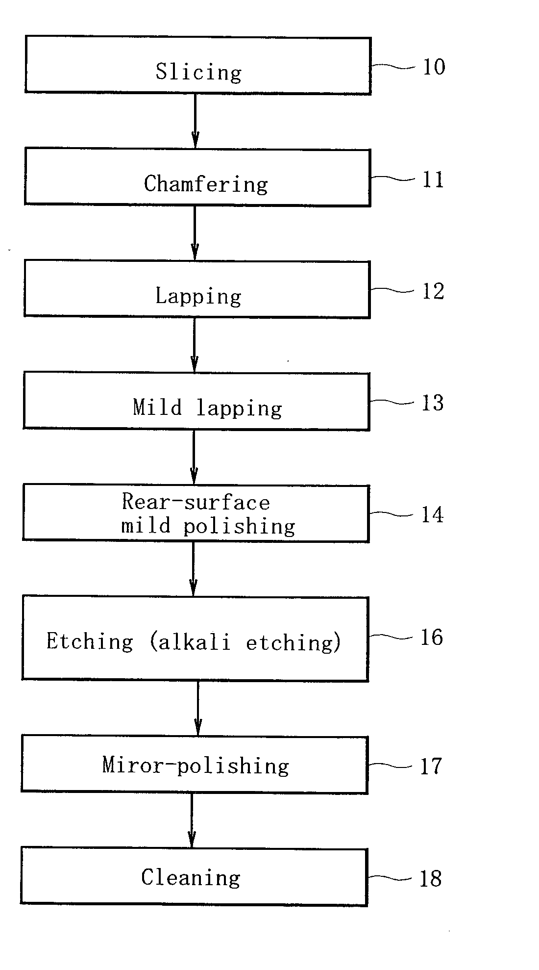
[0019] Next, the embodiments of the invention will be described with reference to accompanying drawings.

[0020] At first, a single-crystal silicon ingot grown has its front and rear ends removed to produce a silicon cylindrical mass. Then, to make the cylindrical mass uniform in its diameter, the periphery of the silicon mass is scraped to give a silicon block body having a uniform diameter. An orientation flat or orientation notch is formed on the block body to indicate the orientation of crystal in the block. After the processing, as shown in FIG. 1, the block body is sliced with a specified angle with respect to the central axis of the block body (step 10).

[0021] Each wafer obtained as a result of slicing is chamfered on its periphery to prevent the development of notches and flaws there (step 11). This chamfering step can prevent the occurrence of crown phenomenon or the abnormal development of an annular ridge which would otherwise occur along the periphery of a wafer when the...


PUM

PropertyMeasurementUnit
timeaaaaaaaaaa
total thicknessaaaaaaaaaa
thicknessaaaaaaaaaa

Abstract

Provided is a method for producing a silicon wafer those surfaces exhibit precise flatness and minute surface roughness, and which allows one to visually discriminate between the front and rear surfaces, the method comprising a slicing step of slicing a single-crystal ingot into thin disc-like wafers, a chamfering step of chamfering the wafer, a lapping step for flattening the chamfered wafer, a mild lapping step for abrading away part of processing distortions on the rear surface of the wafer left after chamfering and lapping, a rear-surface mild polishing step for abrading away part of roughness on the rear surface of the wafer, an etching step for alkali-etching the remains of processing distortions on the front and rear surfaces of the wafer, a mirror-polishing step for mirror-polishing the surface of the etched wafer, and a cleaning step for cleaning the mirror-polished wafer.

Description

BACKGROUND OF THE INVENTION [0001] 1. Field of the Invention [0002] The present invention provides a method for producing a silicon wafer whereby it is possible to fabricate a wafer both of whose surfaces exhibit a high precision flatness and minute surface roughness, and which allows one to visually discriminate between the front and rear surfaces of the wafer. [0003] 2. Description of the Related Art [0004] The conventional method for producing a semiconductor silicon wafer comprises the steps of separating a silicon block from a silicon single-crystal ingot pulled upward, slicing the silicon block to produce wafers, subjecting the wafer to chamfering, mechanical polishing (lapping), etching and mirror polishing (polishing), and cleaning the wafer. Thus, a wafer is obtained that has a high precision flatness. The steps constituting the conventional method may be modified in various manners depending on given purposes: some foregoing steps may be exchanged in order for other later ...

Claims


Application Information

Patent Timeline
07 Jul 2005
Publication
US20050148181A1
IPC
H01L21/304; B24B37/04; H01L21/302; H01L21/306; H01L21/461
CPC
B24B37/042; C30B29/06; H01L21/30608; H01L21/02019; H01L21/30604; C30B33/10
Inventors
KOYATA, SAKAE; TAKAISHI, KAZUSHIGE