Method for determining the construction of a mask for the micropatterning of semiconductor substrates by means of photolithography

a technology of semiconductor substrates and construction methods, applied in the field of determining the construction of masks by means of photolithography, can solve the problems of high computational complexity, difficult to develop new photolithography solutions, and masks with simple geometries can be analyzed in this way, and achieve the effect of precise determination of the construction of masks

Inactive Publication Date: 2005-07-07
POLARIS INNOVATIONS LTD
View PDF17 Cites 28 Cited by
  • Summary
  • Abstract
  • Description
  • Claims
  • Application Information

AI Technical Summary

Benefits of technology

[0053] The computer program improved according to the invention results in a truer-to-reality and more precise determination of the construction of a mask compared with the known methods for determining the construction of a mask for the micropatterning of semiconductor substrates by means of photolithography. Furthermore, the computer program improved according to the invention also makes it possible to determine extensive and complex masks which conventional methods were unable to stimulate.

Problems solved by technology

Due to the high computational complexity, only masks with simple geometries can be analyzed in this way.
This makes it more difficult to develop new photolithography solutions and has hitherto precluded the application of photolithography simulations for the optical proximity correction methods.
A moderate improvement is possible as a result, but the transmission factor depends very greatly on the mask goemetry and it is therefore very difficult to generalize the method for general mask goemetries.
An unsatisfactory simulation result is often produced in the case of mask geometries which deviate from the mask geometries used for determining the transmission factor.

Method used


Image

  • Method for determining the construction of a mask for the micropatterning of semiconductor substrates by means of photolithography
  • Method for determining the construction of a mask for the micropatterning of semiconductor substrates by means of photolithography
  • Method for determining the construction of a mask for the micropatterning of semiconductor substrates by means of photolithography

Examples


Embodiment Construction

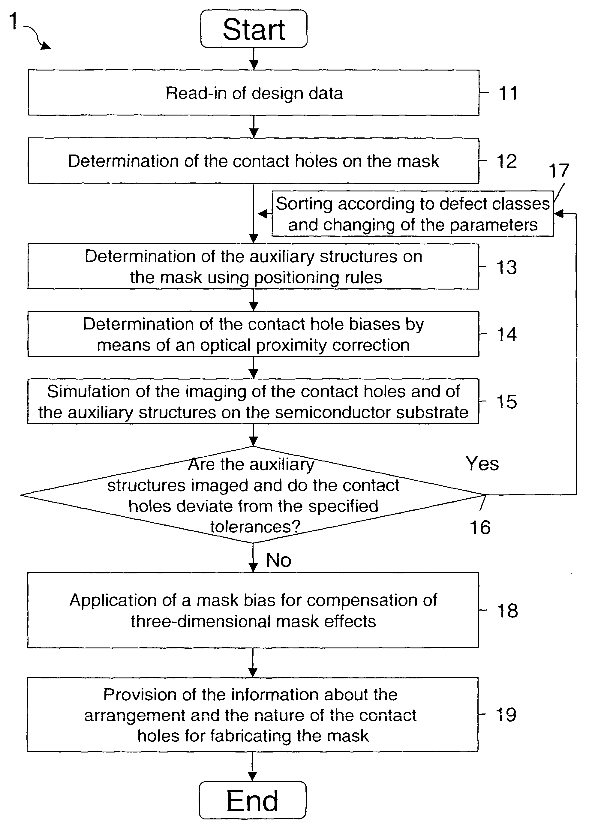
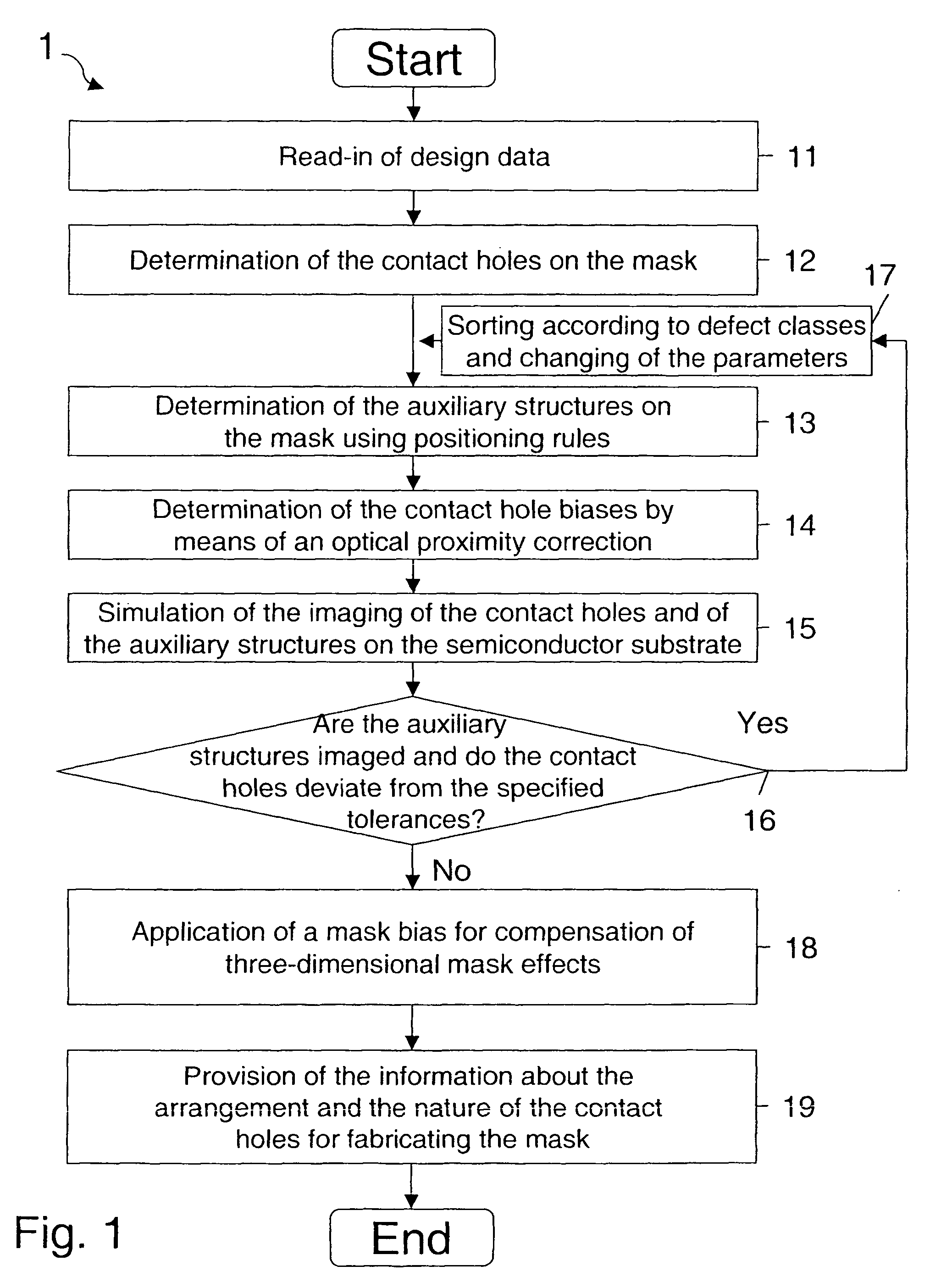
[0075]FIG. 1 shows a first flow diagram 1 for illustrating the method steps 11 to 19 of a first method according to the invention for determining the construction of a mask.

[0076] In this case, the method steps 11 to 19 are carried out exclusively on a computer system that is not represented in FIG. 1. An image of a mask is created and optimized on the computer system below. In this case, mask image is understood to mean the description of the real mask by means of data, said description being created on the computer system.

[0077] In the first method step 11, design data are read into a main memory area of the computer system. In this case, the design data represent the surface structure to be produced on the semiconductor substrate, in particular on the semiconductor wafer. In this case, the design data comprise a plurality of planes, precisely one plane being selected for the method according to the invention. This plane is the contact plane of the semiconductor substrate. The c...


PUM

PropertyMeasurementUnit
refractive indexaaaaaaaaaa
thicknessaaaaaaaaaa
thicknessaaaaaaaaaa

Abstract

In the method, which is to be carried out on a computer system, firstly design data of a semiconductor substrate are read in and, on the basis thereof, a mask image is generated in the form of a data structure with contact holes and with auxiliary structures on the computer system. Afterwards, contact hole biases are determined by means of an optical proximity correction method and the relevant contact holes are corrected on the basis of these contact hole biases. By means of subsequent imaging simulation of the mask image on the semiconductor substrate, undesired imaging auxiliary structures and contact holes deviating from specified tolerances on the semiconductor substrate are detected and corrected. During the imaging simulation of the mask image, a mask bias is employed in order to compensate for three-dimensional mask effects. A real mask can be produced on the basis of the mask image thus determined.

Description

CROSS-REFERENCE TO RELATED APPLICATION [0001] This application is a continuation of copending International Application No. PCT / DE03 / 02160 filed Jun. 30, 2003 which designates the United States, and claims priority to German application no. 102 30 532.3 filed Jul. 5, 2002.TECHNICAL FIELD OF THE INVENTION [0002] The present invention relates to a method for determining the construction of a mask for the micropatterning of semiconductor substrates by means of photolithography. DESCRIPTION OF RELATED ART AND BACKGROUND OF THE INVENTION [0003] In the fabrication of semiconductor components, photolithography is often used for the micropatterning of a semiconductor substrate. The task of the photolithography is to transfer structures from a photomask to a semiconductor substrate. In accordance with a basic concept of photolithography, desired regions of a radiation-sensitive photoresist layer on the semiconductor substrate are irradiated in such a way that only the irradiated or only the ...

Claims


Application Information

Patent Timeline
Patent Type & Authority Applications(United States)
IPC IPC(8): G03F1/00G03F1/36
CPCG03F1/36G03F1/144
Inventor KOEHLE, RODERICKPUFALL, REINHARD
Owner POLARIS INNOVATIONS LTD
Why Eureka
Try Eureka