Method of manufacturing a thin film transistor, thin film transistor, thin film transistor circuit, electronic device, and electronic apparatus

Active Publication Date: 2005-07-14
E INK CORPORATION
12 Cites 128 Cited by

AI-Extracted Technical Summary

Problems solved by technology

However, the vacuum deposition method requires a large-scale facility, and presents proble...

Method used

[0063] The source electrode 3 and drain electrode 4 are provided on the substrate 2 in the channel length L direction side by side with a predetermined distance. As a material for forming the source electrode 3 and the drain electrode 4, a material that can be deposited by an electroless plating process described below. Specifically, for each of materials composing the source electrode 3 and the drain electrode 4, Ni, Cu, Co, Au, Pd, or materials composed mainly of alloys including these metals are preferably used. By forming the source electrode 3 and the drain electrode 4 with these metal materials, the performance of the thin film transistors 1 can further be enhanced.
[0067] Further, on the substrate 2, there is provided the organic semiconductor layer 5 so as to cover the source electrode 3 and the drain electrode 4. The organic semiconductor layer 5 is made mainly of an organic semiconductor material (an organic material presenting with an electrically conductive property similar to a semiconductor material). The organic semiconductor layer 5 is preferably arranged substantially parallel to the channel length L direction at least in a channel region 51. According to this structure, the carrier mobility in the channel region 51 is increased resulting in the faster operational speed of the thin film transistor 1.
[0069] The polymeric organic semiconductor materials can be formed as films by simple processes, and easily arranged in predetermined directions. Further, in these materials, materials made mainly of at least one of fluorene-bithiophen copolymer, polyarylamine, or derivatives of the two are preferably used as polymeric organic semiconductor materials (conjugated polymeric materials) for the reasons of the oxidation resistance and the stability in the air.
[0073] The gate insulating layer 6 is provided on the organic semiconductor layer 5. The gate insulating layer 6 is provided for insulating the gate electrode 7 from the source electrode 3 and the drain electrode 4. The gate insulating layer 6 is preferably composed mainly of an organic material (in particular an organic polymeric material). The gate insulating material 6 composed mainly of an organic polymeric material is easy to be formed, and capable of enhancing adhesiveness with the organic semiconductor layer 5.
[0075] The thickness (in average) of the gate electrode 6 is not particularly limited, but is preferably in a range of about 10 through 5000 nm, and is further preferably in a range of about 100 through 1000 nm. By arranging the thickness of the gate electrode 6 within the range described above, the thin film transistor 1 can be prevented from becoming larger (in particular, increasing the thickness thereof) while surly insulating the source electrode 3 and the drain electrode 4 from the gate electrode 7.
[0088] [A1-I] Firstly, the substrate 2 as shown in FIG. 2A is provided and then washed by, for example, water (purified water) and/or organic solvent alone or in combination. According to the above, the wettability of the substrate 2 to water is improved to easily contact with various processing fluids shown below.
[0090] The process (surface roughening) for enhancing the adhesiveness is executed by etching the surface of the substrate 2 with the etching fluid and then treating with processing fluid including a reducing agent.
[0092] Meanwhile, the reducing agent used for the processing fluid is not particularly limited, but is preferably selected from those substantially free of alkali metals. According to the above, since no alkali metal ions is captured to the surface of the substrate 2, the alkali metal ions are prevented from diffusing to (interfusing in) the organic semiconductor layer 5 formed in a process executed later, and as a result, deterioration of the performance of the organic semiconductor layer 5 can be prevented.
[0117] As the reducing agent, for example, hydrazine, ammonium hypophosphite, and so on can be cited. Among these agents, those composed mainly of at least one of hydrazine and ammonium hypophosphite are more preferable. By using these materials as the reducing agent under appropriate plating solution temperature and appropriate plating solution pH, the speed of forming the plated film 8 is made proper, which makes it easy to control the thickness of the film within the optimum range of the film thickness required to the source electrode 3 and the drain electrode 4.
[0122] It is preferable that a pH adjuster (a pH buffer) is further mixed (added) to such a plating solution 10. According to the above, it is prevented or controlled that the pH of the plating solution 10 is lowered as electroless plating proceeds, and as a result, slow-down of the deposition rate or changes in composition or characteristics of the plated film 8 can effectively be prevented.
[0125] The process time of the substrate 2 in the plating solution 10 is preferably in a range of about 10 seconds through 5 minutes, and further preferably in a range of about 20 seconds through 3 minutes. If the pH and the temperature of the plating solution 10 and the process time by the plating solution 10 are arranged within the ranges mentioned above, the deposition rate becomes especially proper, and accordingly the plated film 8 having an even thickness can be formed with high precision.
[0130] [A1-VII] And then, by removing the resist layer 9, the source electrode 3 and the drain electrode 4 as shown in FIG. 3F can be obtained. Although resist removing fluid is preferably used for removing the resist layer 9, other methods such as, for example, the physical etching methods mentioned above can also be used. As described above, by using the photolithography method and the etching method in combination, the source electrode 3 and the drain electrode 4 with high dimensional accuracy can easily and surely be formed.
[0131] Therefore, the distance (the channel length L) between the source electrode 3 and the drain electrode 4 can be set to be comparatively shorter, thus providing the thin film transistor 1 with low absolute value of the threshold voltage and large drain current, namely excelling at characteristics necessary for switching elements. Note that either of a negative type of resist material and a positive type of resist material can be used as the resist material of the photolithography method.
[0133] Subsequently, the substrate 2 having the source electrode 3 and the drain electrode 4 formed thereon is washed using, for example, water (purified water or the like) and/or organic solvents alone or in combination. And then, as shown in FIG. 4G, any organic matters existing on the surface of the substrate 2, on which the organic semiconductor layer 5 is to be formed, are removed. Thus, the barrier for the carrier in the interface between the organic semiconductor layer 5 and the source electrode 3, the drain electrode 4 can be removed to improve the characteristics of the thin film transistor 1.
[0134] As the method (the removing method) of removing organic matters, for example, a plasma process, a process with ozone water, etching with an acid or an alkali, mechanical removal of the surface layer, and UV (in particular, deep UV) radiation can be cited, and one or more of these processes can be used alone or in combination. Among these processes, the plasma process is preferable as the method of removing the organic matters. According to the plasma process, the organic matters can surely be removed in a short period of time.
[0135] When executing the plasma process, the substrate 2 is carried in a chamber equipped with a decompression means and a plasma generation means, and can be processed by generating plasma in the chamber in a decompressed condition, or by ejecting plasma against the surface of the substrate from a head equipped with a plasma ejection nozzle. According to the latter method, since the plasma process can be executed in the atmospheric pressure, the chamber and the decompression means can be omitted to provide advantages of a low manufacturing cost and a short turn around time in manufacturing.
[0136] In the conditions of the atmospheric pressure plasma, for example, the gas flow rate is in a range of about 10 through 300 sccm, and the RF power is in a rang...

Benefits of technology

[0038] A thin film transistor circuit according to the present invention comprises the thin film transistor according to the present invention. Thus, the thin film transistor circuit with high reliability can be obtained.
[0039] An electronic device according to the present invention comprises the thin film transist...

Abstract

Aspects of the invention can provide a method of manufacturing a thin film transistor capable of manufacturing a high-performance thin film transistor with a simple process, a thin film transistor manufactured using the method of manufacturing a thin film transistor, and a thin film transistor circuit, an electronic device, and an electronic apparatus each equipped with the thin film transistor. The method of manufacturing a thin film transistor according to the invention can include the first step of forming a source electrode and a drain electrode on a substrate by an electroless plating process, the second step of forming an organic semiconductor layer in at least an area between the source electrode and the drain electrode using a costing method, the third step of forming a gate insulating layer on the organic semiconductor layer using a coating method, and the fourth step of forming a gate electrode using a coating method so as to overlap an area on the gate insulating layer and between the source electrode and the drain electrode.

Application Domain

Technology Topic

Image

  • Method of manufacturing a thin film transistor, thin film transistor, thin film transistor circuit, electronic device, and electronic apparatus
  • Method of manufacturing a thin film transistor, thin film transistor, thin film transistor circuit, electronic device, and electronic apparatus
  • Method of manufacturing a thin film transistor, thin film transistor, thin film transistor circuit, electronic device, and electronic apparatus

Examples

  • Experimental program(5)

Example

EXAMPLE 1
[0218] Firstly, a glass substrate with a thickness of 1 mm is provided, and washed with water (cleaning fluid). Then, the glass substrate is dipped in an aqueous solution (25° C.) of distearyl dimethyl ammonium chloride (cationic surface-active agent) for 60 seconds. Thus, distearyl dimethyl ammonium chloride is absorbed on the surface of the glass substrate. Subsequently, the glass substrate is washed with water.
[0219] Then, the glass substrate is dipped in a Sn-Pd colloidal suspension (25° C.) for 60 seconds. Thus, Sn-Pd is absorbed on the surface of the glass substrate. Subsequently, the glass substrate is washed with water. Then, the glass substrate is dipped in an aqueous solution (25° C.) including HBF4 and glucose for 60 seconds. Thus, Sn is removed from the surface of the glass substrate to expose Pd on the surface of the glass substrate. Subsequently, the glass substrate is washed with water.
[0220] Then, the glass substrate is dipped in a Ni plating solution (80° C., pH 8.5) for 60 seconds. Thus, a Ni plated film with a thickness of 100 nm is formed on the surface of the glass substrate. Note that the Ni plating solution is prepared by dissolving 10 g of nickel sulfate, 100 g of hydrazine (a reducing agent), 5 g of ammonium sulfide (a pH adjuster) with 1 L of water.
[0221] And then, a resist layer patterned correspondingly to the shapes of the source electrode and the drain electrode is formed on the Ni plated film by a lithography process. Note that “OPR800” produced by Tokyo Ohka Kogyo Co., Ltd is used as the resist material. And then, the glass substrate is dipped in an aqueous solution (25° C.) of iron chloride. Thus, the plated film not covered by the resist layer is removed to form the source electrode and the drain electrode. It should be noted that the distance (the channel length L) between the source electrode and the drain electrode is arranged to be 20 μm, and the channel width W is arranged to be 1 mm.
[0222] Then, after removing the resist layer using the resist remover, the glass substrate with the source electrode and the drain electrode formed thereon is sequentially washed with water and methanol. And then, the oxygen plasma process (the atmospheric pressure oxygen plasma process) is executed on the substrate with the source electrode and the drain electrode formed thereon under the atmospheric pressure. It should be noted that, in the conditions of the atmospheric pressure plasma process, the RF power is set to be 0.05 W/cm2 and the flow rate is set to be 80 sccm.
[0223] Subsequently, a 1% (wt/vol) toluene solution of F8T2 (fluorene-bithiophene copolymer) is coated on the glass substrate by the spin coating process (2400 rpm), and then dried at 60° C. for 10 minutes. Thus, the organic semiconductor layer with an average thickness of 50 nm is formed. And then, a 5% (wt/vol) butyl acetate solution of polymethylmethacrylate (PMMA) is coated on the organic semiconductor layer by the spin coating process (2400 rpm), and then dried at 60° C. for 10 minutes. Further, a 2% (wt/vol) isopropyl alcohol solution of polyvinylphenol is coated thereon by the spin coating process (2400 rpm), and then dried at 60° C. for 10 minutes. Thus, the gate insulating layer with an average thickness of 500 nm is formed. And then, a water dispersion (viscosity of 5 cps at room temperature) of PEDOT (poly-ethylenedioxythiophene) is coated on the gate insulating layer in an area corresponding to the region between the source electrode and the drain electrode by the inkjet process (20 pL droplet), and then dried at 80° C. for 10 minutes. Thus, the gate electrode with an average thickness of 100 nm is formed. The thin film transistor shown in FIGS. 1A and 1B is manufactured through the steps described above.

Example

EXAMPLE 2 THROUGH 9
[0224] The thin film transistor shown in FIGS. 1A and 1B is manufactured similarly to the example 1 while changing the nature of the reducing agent, the nature of the pH adjuster, and presence or absence and/or the nature of the plasma process as shown in TABLE 1. TABLE 1 Reducing agent pH adjuster Plasma process Example 1 Hydrazine Ammonium sulfide Atmospheric pressure oxygen plasma Example 2 Ammonium Ammonium sulfide Atmospheric pressure hypophosphite oxygen plasma Example 3 Hydrazine + Ammonium Ammonium sulfide Atmospheric pressure hypophosphite*1 oxygen plasma Example 4 Hydrazine Ammonia water Atmospheric pressure oxygen plasma Example 5 Hydrazine Trimethyl Atmospheric pressure ammonium hydride oxygen plasma Example 6 Hydrazine Ammonium sulfide + Trimethyl Atmospheric pressure ammonium hydride*2 oxygen plasma Example 7 Hydrazine Ammonium sulfide Atmospheric pressure Ar plasma Example 8 Hydrazine Ammonium sulfide Atmospheric pressure CF4 plasma Example 7 Hydrazine Ammonium sulfide No Example 8 Ammonium Ammonium sulfide No hypophosphite Example 9 Hydrazine + Sodium Ammonium sulfide Atmospheric pressure hypophosphite*3 oxygen plasma Example 10 Hydrazine Ammonium sulfide Atmospheric pressure oxygen plasma Example 11 Hydrazine Ammonium sulfide Atmospheric pressure oxygen plasma Example 12 Hydrazine Ammonium sulfide Atmospheric pressure oxygen plasma
*1Hydrazine:Ammonium hypophosphite = 60:40 (weight ratio)
*2Ammonium sulfide:Trimethyl ammonium hydride = 70:30 (weight ratio)
*3Hydrazine:Sodium hypophosphite = 90:10 (weight ratio)

Example

EXAMPLE 10
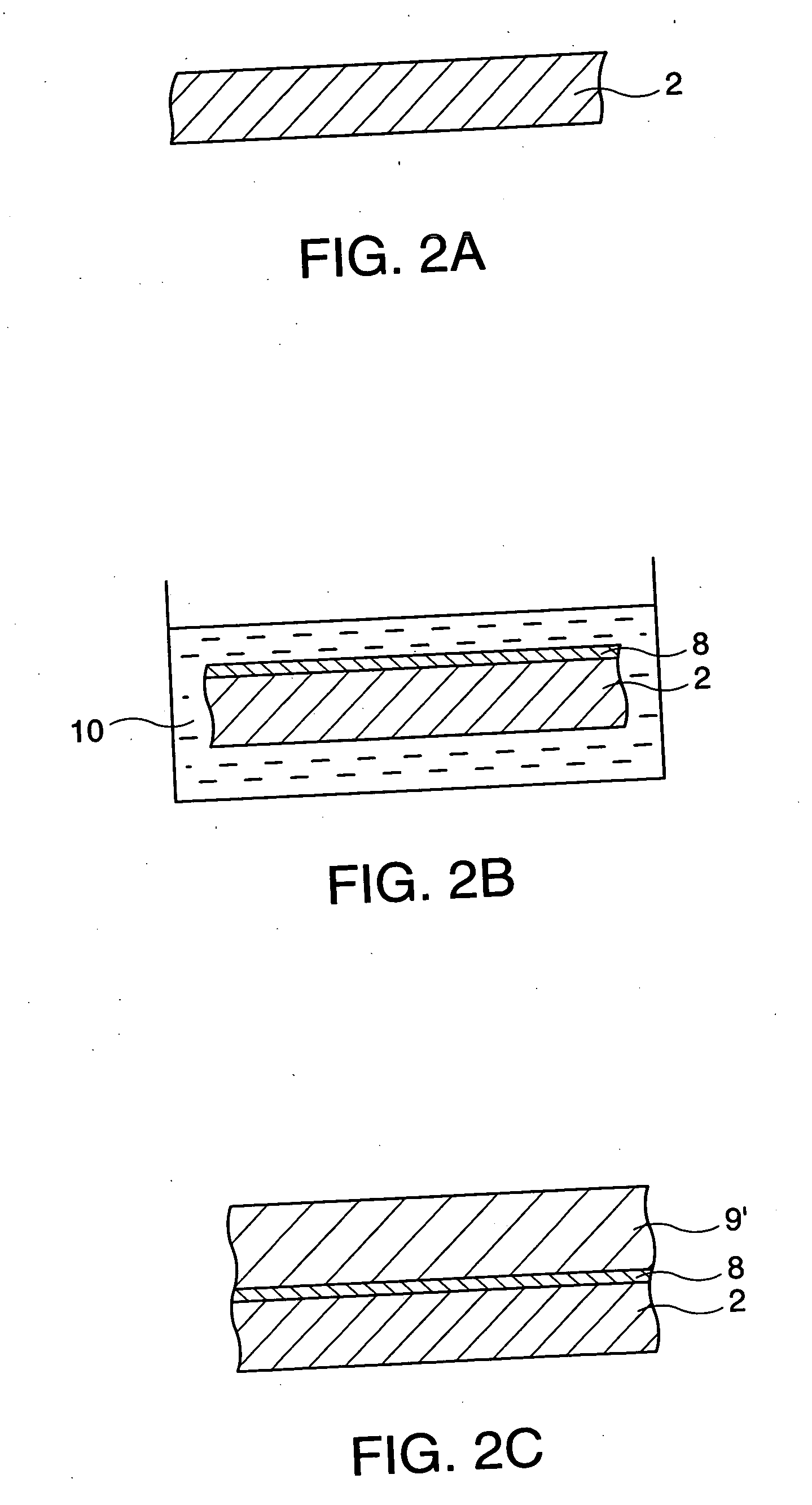
[0225] Firstly, a polyimide substrate with a thickness of 35 μm is provided, and washed with water (cleaning fluid). Subsequently, the polyimide substrate is dipped in an aqueous solution (25° C.) including CrO3 and sulfuric acid for 60 seconds, and then dipped in an aqueous solution (25° C.) of ammonium sulfite hydrate 60 seconds as a pre-process.
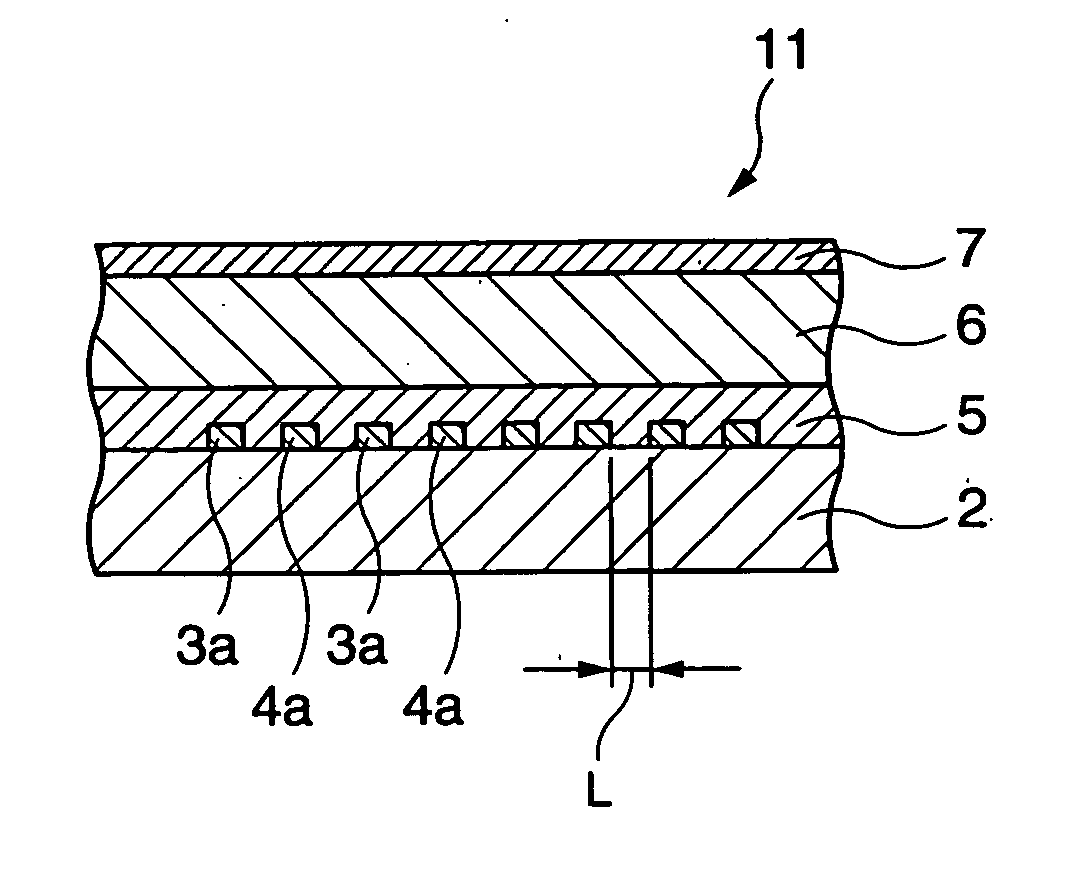
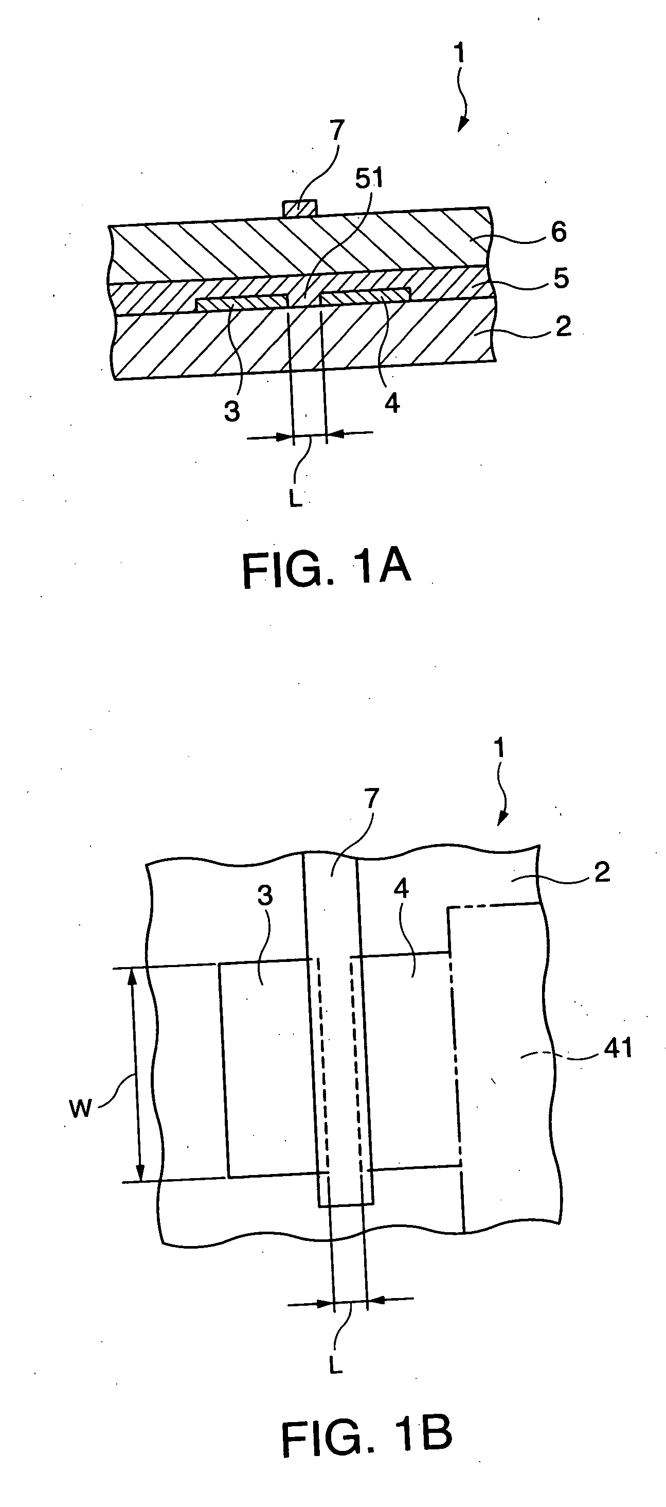
[0226] And then, a resist layer having a pattern corresponding to the area other than the area in which the source electrode and the drain electrode are to be formed is formed on the polyimide substrate by a lithography process. Note that “PMERP-NZ30” produced by Tokyo Ohka Kogyo Co., Ltd is used as the resist material. Then, the plated film is formed similarly to the example 1. Note that the distance (the channel length L) between the source electrode and the drain electrode is arranged to be 20 μm, and the channel width W is arranged to be 1 mm.
[0227] Then, after removing the resist layer using the resist remover, the polyimide substrate with the source electrode and the drain electrode formed thereon is sequentially washed with water and methanol. And then, the oxygen plasma process (the atmospheric pressure oxygen plasma process) is executed thereon under the atmospheric pressure similarly to the example 1. Subsequently, the organic semiconductor layer, the gate insulating layer, and the gate electrode are respectively formed on the polyimide substrate similarly to the example 1.
[0228] The thin film transistor shown in FIGS. 1A and 1B is manufactured through the steps described above.

PUM

PropertyMeasurementUnit
Pressure
Electrical conductivity
Adhesivity
tensileMPa
Particle sizePa
strength10

Description & Claims & Application Information

We can also present the details of the Description, Claims and Application information to help users get a comprehensive understanding of the technical details of the patent, such as background art, summary of invention, brief description of drawings, description of embodiments, and other original content. On the other hand, users can also determine the specific scope of protection of the technology through the list of claims; as well as understand the changes in the life cycle of the technology with the presentation of the patent timeline. Login to view more.

Similar technology patents

Classification and recommendation of technical efficacy words

Why Eureka
Try Eureka