

Semiconductor device and method of manufacturing the same
a technology of semiconductor devices and semiconductors, applied in semiconductor devices, semiconductor/solid-state device details, electrical apparatus, etc., can solve the problems of low-k film strength, film cracking, and structure to be unstabl
- Summary
- Abstract
- Description
- Claims
- Application Information
AI Technical Summary
Benefits of technology
Problems solved by technology
Method used
Image

Examples
first embodiment
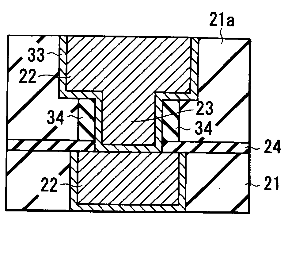
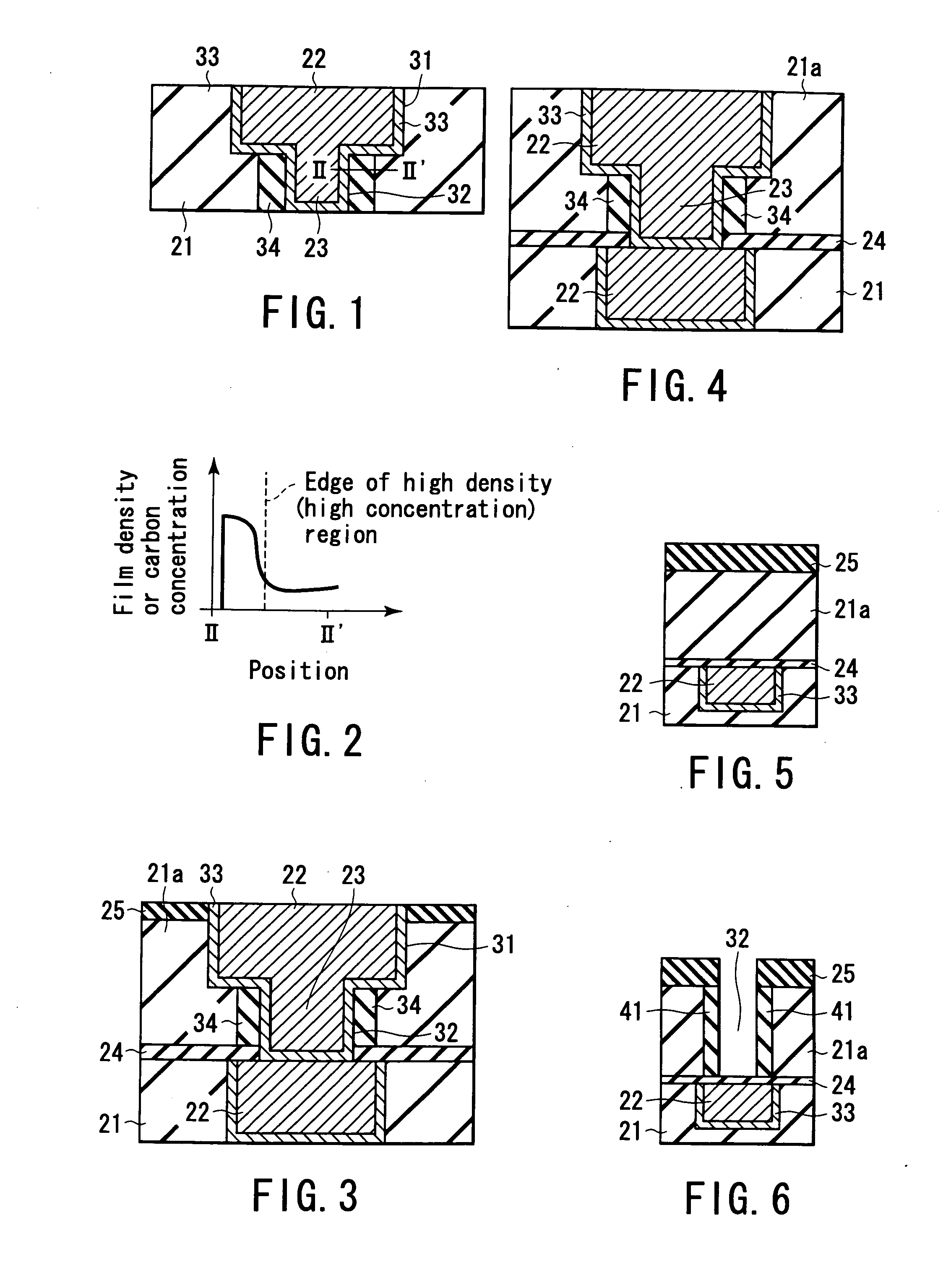
[0038]FIG. 1 is a cross-sectional view schematically showing a semiconductor device according to a first embodiment of the present invention. FIG. 1 shows a part of the semiconductor device having multi-layer interconnection structure. As shown in FIG. 1, an interlayer insulating film 21 is formed containing a porous insulating film. More specifically, SiOC film having dielectric constant k not greater than 2.7 is used as the interlayer insulating film 21. In addition, the following organic polymers (organic polymer films) containing SiOH in place of SiOC may be used. The organic polymers are methyl siloxane, methyl silsesquioxane (MSQ), poly allylene hydrocarbon and benzyoxazole, etc. The interlayer insulating film 21 is formed of a stacked layer of non-low-dielectric (non-low-k) films such as SiO2 and SiC.
[0039] The interlayer insulating film 21 is formed with interconnection trench 31 and via hole 32. The interconnection trench 31 and the via hole 32 are filled with conductive m...
second embodiment
[0062] According to the second embodiment, the interlayer insulating film 21 is formed of two kinds of low-k films or more.
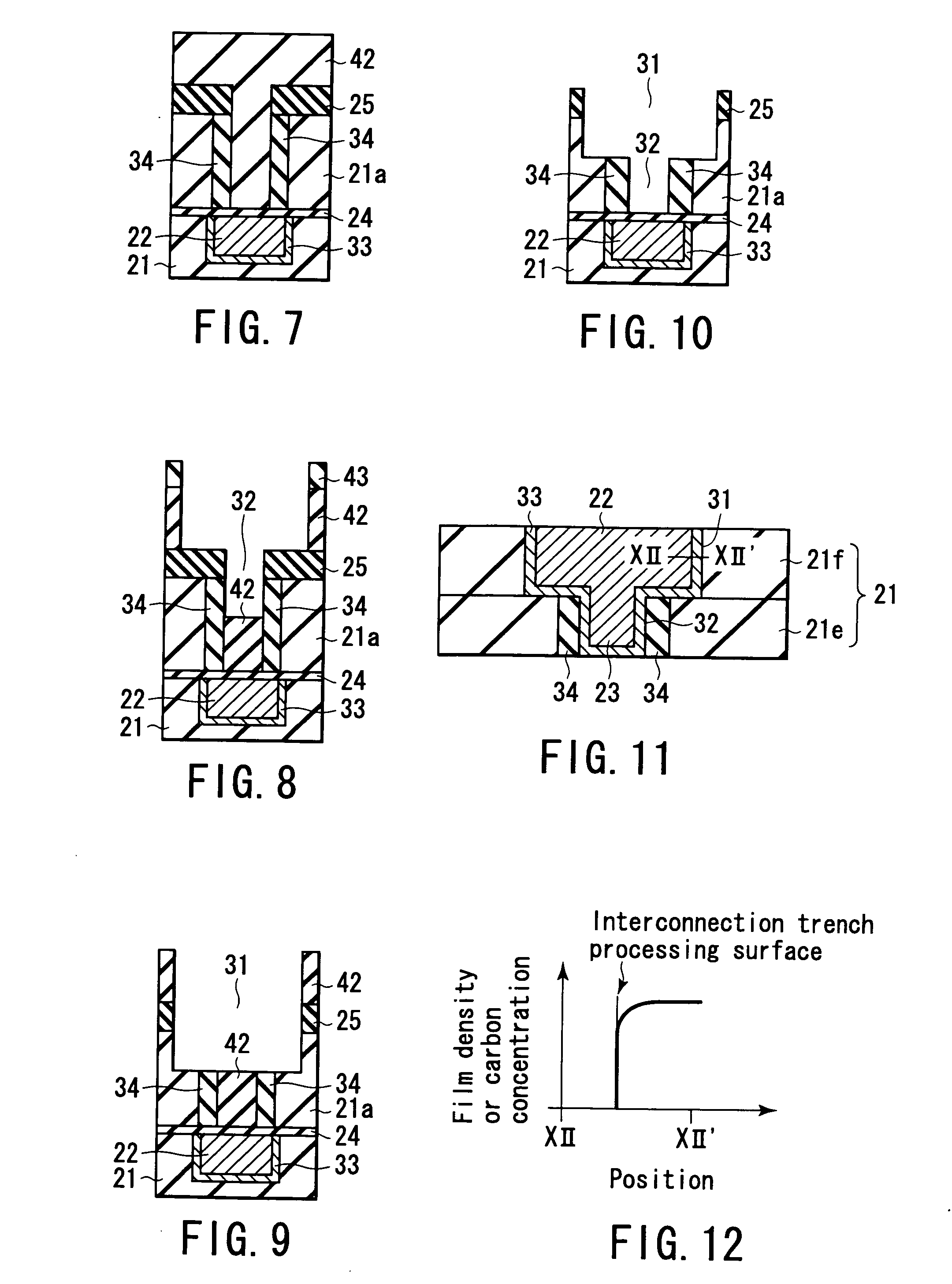
[0063]FIG. 11 is a cross-sectional view schematically showing a part of a semiconductor device according to the second embodiment of the present invention. As shown in FIG. 11, the interlayer insulating film 21 is composed of interlayer insulating films 21e and 21f. The interlayer insulating film 21e consists of methyl siloxane or methyl silsesquioxiane having dielectric constant k not greater than 2.7. The interlayer insulating film 21f consists of organic polymer having dielectric constant k not greater than 2.7. Either of the interlayer insulating films 21e and 21f may be used as the bottom layer. FIG. 11 shows the case where the interlayer insulating films 21e is used as the bottom layer. The interlayer insulating films 21e and 21f have the same features as the interlayer insulating film 21 described in the first embodiment.
[0064] The boundary between inte...
third embodiment
[0080] The third embodiment relates to another method of manufacturing the semiconductor device having the structure described in the second embodiment.
[0081]FIG. 24 to FIG. 29 show the third embodiment of the present invention, and are cross-sectional views successively showing the process of manufacturing the semiconductor device according to the second embodiment. As shown in FIG. 24, the lower interlayer insulating film 21 is formed above a semiconductor substrate (not shown). The surface of the interlayer insulating film 21 is formed with the interconnection 22 via the barrier metal 33. The stopper film 24, interlayer insulating film 21e and cap film 25 are successively deposited on the interlayer insulating film 21 by CVD or coating process. Thereafter, hard mask films 53 and 54 are successively formed on the cap film 25.
[0082] As illustrated in FIG. 25, a resist film 55 having a hole opening corresponding to the interconnection trench 31 is formed on the hard mask film 54. ...
PUM
 Abstract
Description
Claims
Application Information