Method and device for testing a sense amp

a technology of sense amp and circuit device, which is applied in the direction of information storage, static storage, digital storage, etc., can solve the problems of slow down of additional digit line voltage, errors in reading, and saturated current in the resistor, so as to improve the ability of sense amp, faster reading speed, and quick test of memory arrays

Inactive Publication Date: 2005-07-14
MICRON TECH INC
View PDF28 Cites 0 Cited by
  • Summary
  • Abstract
  • Description
  • Claims
  • Application Information

AI Technical Summary

Benefits of technology

[0016] In one set of applications involving the regulation of a sense amp, the connection device comprises a sense amp's voltage pulling transistor. Any circuit embodiment covered by the present invention can be used to test drive the transistor. In a preferred method of use, a test data pattern is entered and the data is read several times, with a different voltage driving the sense amp's pulldown transistor each time. One advantage of this preferred method is that it reduces the need for entering several elaborate test data patterns and, therefore, allows for quicker testing of memory arrays. A second advantage is that the embodied method and devices allow a determination of the lowest supply voltage that can be used during normal operation without errors in reading data. Yet another advantage is the ability to determine the highest supply voltage, and therefore the fastest reading speed, that can be used during normal operations without causing capacitive coupling. In doing so, the preferred circuit embodiments and method increase the sense amp's ability to distinguish between a logic 0 voltage and a logic 1 voltage without physically altering the sense amp. Further, in the process of determining the lowest and highest voltages at which the sense amp is capable of functioning, the preferred embodiments and method also provide a way to ascertain the margin without dissecting components of the sense amp.
[0017] Concerning the specific errors that may be detected in relation to equilibrating the digit lines, the connection device comprises an isolation bleeder device coupled between the DVC2 voltage generator and a digit line pair. The circuit embodiments provide a test mode apparatus for driving the bleeder device in order to slow or quicken the equilibration of the digit line pair. Applying these embodiments provides the advantage of a quicker detection of defects such as a short from a digit line to ground, a short from a digit line to a cell plate, and a short within the storage capacitor of a memory cell. The embodiments also provide an alternative advantage of overcoming the influence of these defects during non-test modes.

Problems solved by technology

In doing so, there is a risk that the transistor will become saturated with current and therefore become slower in pulling down the voltage of additional digit lines.
This may lead to errors in reading, especially if an entire row of memory cells is storing logic 1's except for one cell storing a logic 0; for once the logic 0 is discharged, a slow pulldown may result in an improper reading of that logic 0 value.
However, one of ordinary skill in the art will appreciate that this solution requires. a costly metal mask change.
Further, any attempt to speed up the slowed pulldown raises other problems in reading, as disclosed in U.S. Pat. No. 5,042,011, by Casper, et al.
When the sense amp finally turns on, it shorts out the capacitive coupling, bouncing the digit lines and, in the process, creates line noise that will interfere with the ability to read the data properly.
As a result, each row contains only one cell storing a logic 0, thereby creating the most likely circumstance for an error in reading the data.
The problem with this process, however, is that it is time consuming to enter multiple samples of test data.
In addition to inadequate pulldown transistors, other problems, such as defects arising during the processing of semiconductor devices, may contribute to reading errors.
As a result, the potential of that digit line will leak towards 0 volts.
Alternatively, assuming that a logic 1 is properly discharged and sensed, a reading error is still likely: Veq may be so low due to the short that the pullup sense amp may not be able to pull up the digit line's voltage in time to register as a logic 1 for purposes of driving external circuitry.
Further, a reading error occurring after this extended precharge cycle will indicate the nature of the defect—in this case a short in at least one of the digit lines.
However, this testing process can be time consuming.
A second problem that could be detected by altering the equilibration rate of the digit lines involves a short between the cell plate and the digit line.
This will affect the margin between Veq and the voltage corresponding to one of the logic values and thereby increase the likelihood of a reading error.
Such a defect could cause a short within the storage capacitor.
As a result, the capacitor, which should be storing a logic 0, has a longer time to charge to a higher voltage, thereby making an error in the next reading cycle more likely.

Method used


Image

  • Method and device for testing a sense amp
  • Method and device for testing a sense amp
  • Method and device for testing a sense amp

Examples


Embodiment Construction

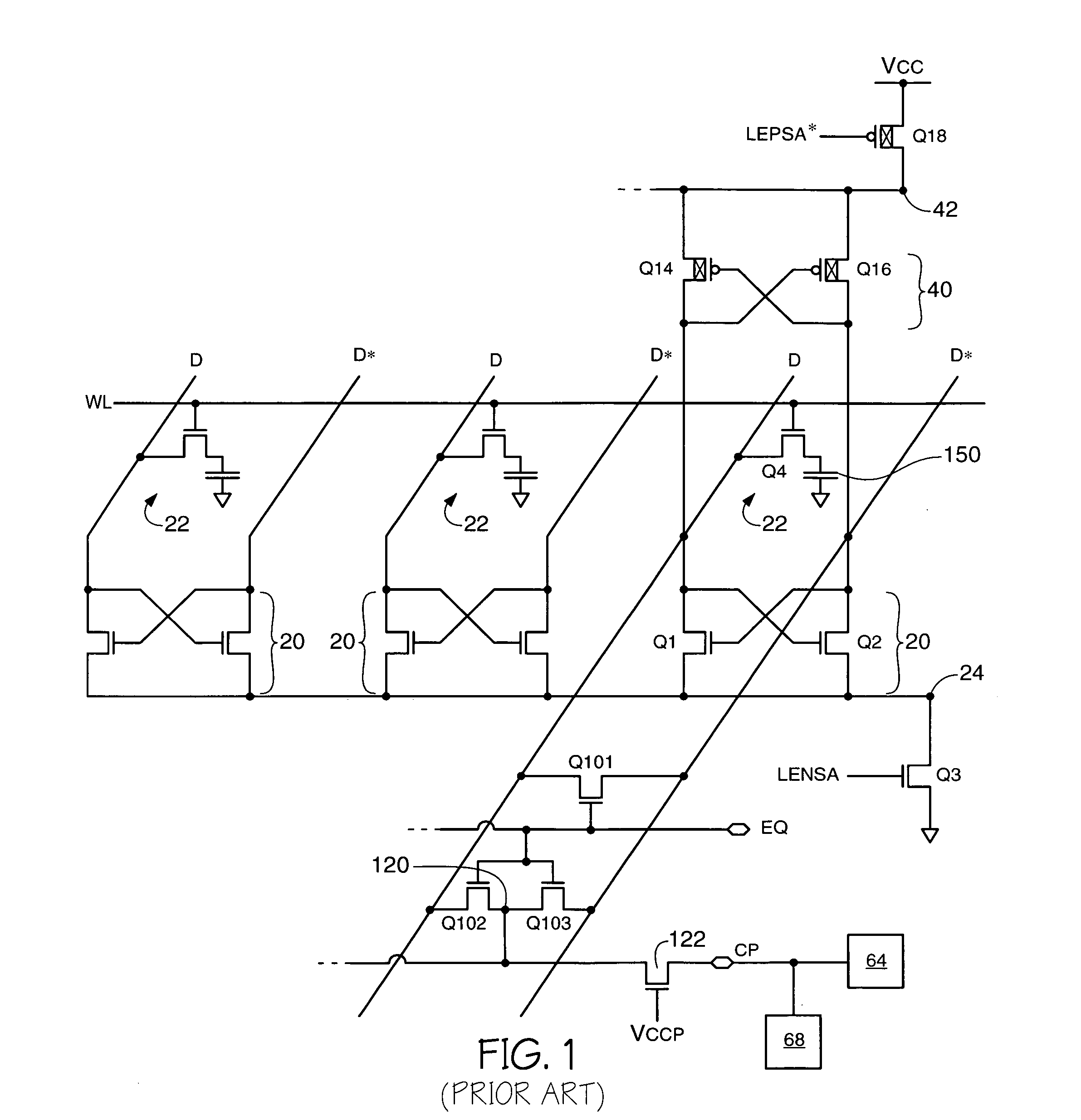
[0035]FIG. 1 illustrates the general configuration of sense amps in a memory array. A pulidown sense amp 20 includes cross coupled n-channel transistors Q1 and Q2, as well as a pulldown transistor Q3, which is an n-channel transistor driven by a signal designated as LENSA, These elements play a part in sensing and amplifying a voltage difference between D and D* caused by shorting a memory cell 22 to D by way of access transistor Q4. The sources of Q1 and Q2 are connected to a common pulldown node 24, and the gate of each is connected to the other's drain. The gate of Q1 also connects to the line D*, whereas the gate of Q2 connects to the line D.

[0036] As discussed above, each line D and its corresponding line D* are initially at the same voltage DVC2. For purposes of explanation, DVC2 is assumed to be 1.65 volts, or one half of the source voltage VCC, which is 3.3 volts. Lines D and D* connect to opposite sides of each sense amp 20. Common pulldown nodes 24 found in the sense amp ...


PUM


Abstract

As pad of a memory array, a circuit is provided for altering the drive applied to an access transistor that regulates electrical communication within the memory array. In one embodiment, the circuit is used to alter the drive applied to a sense amp's voltage-pulling transistor, thereby allowing modification of the voltage-pulling rate for components of the sense amp. A sample of test data is written to the memory array and read several times at varying drive rates in order to determine the sense amp's ability to accommodate external circuitry. In another embodiment, the circuit is used to alter the drive applied to a bleeder device that regulates communication between the digit lines of the memory array and its cell plate. Slowing said communication allows defects within the memory array to have a more pronounced effect and hence increases the chances of finding such defects during testing. The circuit is configured to accept and apply a plurality of voltages, either through a contact pad or from a series of discrete voltage sources coupled to the circuit.

Description

RELATED APPLICATIONS [0001] This application is a continuation of U.S. application Ser. No. 10 / 883,415, filed Jun. 30, 2004; which is a continuation of U.S. application Ser. No. 10 / 608,060, filed Jun. 27, 2003 and issued as U.S. Pat. No. 6,778,452; which is a continuation of U.S. application Ser. No. 10 / 253,844, filed Sep. 23, 2002 and issued as U.S. Pat. No. 6,600,687; which is a continuation of U.S. application Ser. No. 09 / 735,119, filed Dec. 11, 2000 and issued as U.S. Pat. No. 6,469,944; which is a continuation of pending U.S. application Ser. No. 09 / 483,549, filed Jan. 14, 2000 and issued as U.S. Pat. No. 6,181,617; which is a continuation of U.S. application Ser. No. 09 / 260,232, filed on Mar. 1, 1999 and issued as U.S. Pat. No. 6,028,799; which is a divisional of U.S. application Ser. No. 08 / 855,555, filed May 13, 1997 and issued as U.S. Pat. No. 5,877,993.TECHNICAL FIELD [0002] The present invention relates generally to semiconductor circuit devices and, more specifically, to...

Claims


Application Information

Patent Timeline
Patent Type & Authority Applications(United States)
IPC IPC(8): G11C7/00G11C29/02G11C29/12G11C29/44G11C29/48G11C29/50G11C29/56
CPCG11C11/401G11C29/02G11C29/025G11C29/026G11C29/028G11C2029/5004G11C29/44G11C29/48G11C29/50G11C29/50012G11C29/56G11C29/12
Inventor BEIGEL, KURT D.CUTTER, DOUGLAS J.
Owner MICRON TECH INC
Why Eureka
Try Eureka