Method for manufacturing nonvolatile semiconductor memory device

a nonvolatile semiconductor and memory device technology, applied in semiconductor devices, digital storage, instruments, etc., can solve the problems of high consumption power, difficulty in miniaturization, miniaturization and high speed operation, etc., and achieve the effect of high quality, easy adjustment, and high quality of nonvolatile semiconductor memory devices

Inactive Publication Date: 2005-07-14
SHARP KK
View PDF6 Cites 37 Cited by
  • Summary
  • Abstract
  • Description
  • Claims
  • Application Information

AI Technical Summary

Benefits of technology

[0021] According to the manufacturing method of a nonvolatile semiconductor memory device with third aspect, the variable resistive element is formed in such a manner that the variable resistor is placed between the lower electrode and the upper electrode; therefore, a predetermined voltage can be applied between the lower electrode and the upper electrode, so that this voltage can be applied to the variable resistor, changing the resistance value thereof and thereby, the variable resistive element formed of the lower electrode, the variable resistor and the upper electrode can function as a nonvolatile memory element. In addition, a sputtering method where parameters for film growth can be set in a wide range is used for forming the variable resistor; therefore, the formation of a high quality film at a low temperature becomes possible.
[0022] More preferably, in the manufacturing method of a nonvolatile semiconductor memory device according to the third aspect of the present invention, according to a fourth aspect of the present invention, the lower electrode and the upper electrode are formed at a temperature below a temperature, at which the variable resistor is formed, in the process of forming the variable resistive element. As a result, the metal wire that has already been formed can be prevented from being thermally damaged at the temperature, at which the lower electrode and the upper electrode are formed, so that a high quality of nonvolatile semiconductor memory device can be obtained.
[0023] More preferably, in the manufacturing method of a nonvolatile semiconductor memory device according to any of the above aspects of the present invention, according to a fifth aspect of the present invention, the variable resistor is formed at a temperature which is higher than a maximum treatment temperature in a process after formation of the metal wire layer. As a result, the variable resistor film that has been once formed is not annealed at a temperature higher than the film forming temperature; therefore, the initial resistance value that is determined by the film forming temperature can be stably maintained, so that the initial resistance value of the variable resistor can easily be adjusted.

Problems solved by technology

However, these memory devices at the present stage have their merits and demerits, and there is a long way to go before the realization of an ideal “universal memory” which has the respective merits of an SRAM, a DRAM and a flash memory.
The FeRAM, for example, which has already been put into practice, utilizes a spontaneous polarization inversion phenomenon of oxide ferroelectrics and is characterized by a low consumed power and a high speed operation; however, it is inferior due to high cost and destructive readout.
This element has a large problem of high consumed power for magnetization inversion at the time of programming and of a difficulty in miniaturization.
In addition, the OUM based on thermal phase transformation of a chalcogenite material is advantageous in low cost and process matching; however, it has a problem in miniaturization and in a high speed operation due to its thermal operation.

Method used


Image

  • Method for manufacturing nonvolatile semiconductor memory device
  • Method for manufacturing nonvolatile semiconductor memory device
  • Method for manufacturing nonvolatile semiconductor memory device

Examples


Embodiment Construction

[0031] One embodiment of a nonvolatile semiconductor memory device according to the present invention (hereinafter, appropriately referred to as “inventive device”) is described below with reference to the drawings.

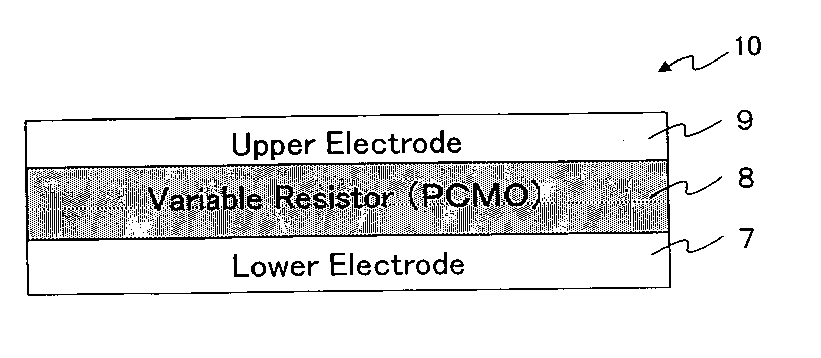
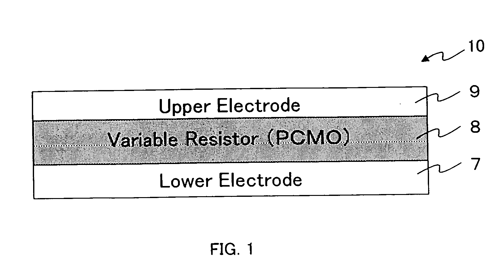
[0032]FIG. 1 is a cross sectional diagram showing the basic structure of a variable resistive element 10 which is a nonvolatile memory element used in an inventive device 100. The basic element structure of variable resistive element 10 is a layered structure where a lower electrode 7, a variable resistor 8 made of a perovskite-type metal oxide film, and an upper electrode 9 are layered in sequence.

[0033] As for the perovskite-type metal oxide that is used as the variable resistor 8, a great number of examples such as Pr1-xCaxMnO3 (PCMO), Pr1-x(Ca,Sr)xMnO3, Nd0.5Sr0.5MnO3, La1-xCaxMnO3, La1-xSrxMnO3 and Gd0.7Ca0.3BaCo2O5+5 are known. Among these, Pr1-xCaxMnO3-based materials, which have a large distortion in the network of the transition metal-oxide bonding and where a ...


PUM


Abstract

In a manufacturing method of a nonvolatile semiconductor memory device including a variable resistive element having a variable resistor made of a perovskite-type metal oxide film, the variable resistor is formed at a temperature which is lower than the melting point of a metal wire layer that has been formed before formation of the variable resistor. More preferably, the variable resistor is formed by a praseodymium calcium manganese oxide, which is represented by a general formula, Pr1-xCaxMnO3, carried out at a film forming temperature in a range from 350° C. to 500° C. according to a sputtering method.

Description

CROSS REFERENCE TO RELATED APPLICATIONS [0001] This Nonprovisional application claims priority under 35 U.S.C. §119(a) on Patent Application No. 2004-004949 filed in Japan on Jan. 13, 2004, the entire contents of which are hereby incorporated by reference. BACKGROUND OF THE INVENTION [0002] 1. Field of the Invention [0003] The present invention relates to a nonvolatile semiconductor memory device and, more specifically, to a manufacturing method of a nonvolatile semiconductor memory device including a variable resistive element having a variable resistor made of a perovskite-type metal oxide film. [0004] 2. Description of the Related Art [0005] In recent years, a variety of device structures such as an FeRAM (Ferroelectric RAM), an MRAM (Magnetic RAM) and an OUM (Ovonic Unified Memory) have been proposed as a next generation nonvolatile random access memory (NVRAM) that makes a rapid operation possible substituting a flash memory, and there has been a fierce competition for the deve...

Claims


Application Information

Patent Timeline
Patent Type & Authority Applications(United States)
IPC IPC(8): H01L27/10G11C13/00H01L21/02H01L21/8246H01L21/8247H01L27/112H01L27/115H01L27/24H01L29/68H01L45/00
CPCG11C13/0007G11C13/003G11C2213/31G11C2213/78G11C2213/79H01L45/147H01L45/1625H01L45/1675H01L27/2436H01L45/04H01L45/1233H01L28/20H10B63/30H10N70/20H10N70/8836H10N70/026H10N70/826H10N70/063
Inventor KAWAZOE, HIDECHIKATAMAI, YUKIOSHIMAOKA, ATSUSHIHAGIWARA, NAOTOMATSUSHITA, YUJINISHI, YUJI
Owner SHARP KK
Why Eureka
Try Eureka