Strained silicon on insulator from film transfer and relaxation by hydrogen implantation

a technology of strained silicon and insulator, applied in the direction of basic electric elements, electrical apparatus, semiconductor devices, etc., can solve the problems of easy propagation of thread dislocations to the topmost strained silicon layer, and achieve the effects of promoting the relaxation of the sige seed layer, better integration, and cost-effectiveness

Active Publication Date: 2005-07-14
SHARP KK
View PDF22 Cites 147 Cited by
  • Summary
  • Abstract
  • Description
  • Claims
  • Application Information

AI Technical Summary

Benefits of technology

[0017] 1. Using a thin relaxed SiGe layer as the strain-induced layer. An additional hydrogen implantation and anneal step is employed to foster the relaxation of the SiGe seed layer. Thus the deposited SiGe layer can be in the range of 250 to 350 nm, much less than the thickness of a few microns reported previously by other inventors. The present invention thin relaxed SiGe layer process offers better integration and is more cost effective.
[0018] 2. In the wafer splitting step using hydrogen implantation, minimization of defects and dislocation in the strained silicon layer by the formation of subsurface microcracks far from the strained silicon layer and under the strain-induced layer. By implanting hydrogen far into the silicon substrate well below the SiGe layer, the threading dislocations do not propagate easily to the topmost strained silicon layer due to the interface of the substrate silicon and the SiGe layer.
[0019] 3. Two step annealing / thinning method for the fabrication of SSOI film transfer. Taking advantage of substrate thinning processes that require much less bonding force of the transfer film on the underlying substrate, a two step annealing / thinning method for SSOI fabrication process is successfully developed to reduce blister or flaking formation of the transfer film. The two step annealing / thinning method basically comprises a first anneal at low temperature for wafer splitting, followed by a dry etch process to reduce the thickness of transfer film without loss of adhesion, before subjected the composite substrate to a second anneal at high temperature and a final CMP or selective wet etch.

Problems solved by technology

By implanting hydrogen far into the silicon substrate well below the SiGe layer, the threading dislocations do not propagate easily to the topmost strained silicon layer due to the interface of the substrate silicon and the SiGe layer.

Method used


Image

  • Strained silicon on insulator from film transfer and relaxation by hydrogen implantation
  • Strained silicon on insulator from film transfer and relaxation by hydrogen implantation
  • Strained silicon on insulator from film transfer and relaxation by hydrogen implantation

Examples


first embodiment

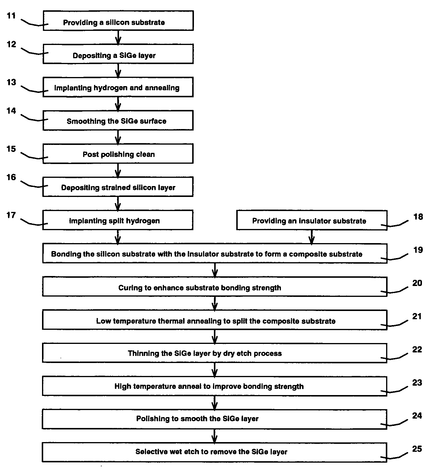
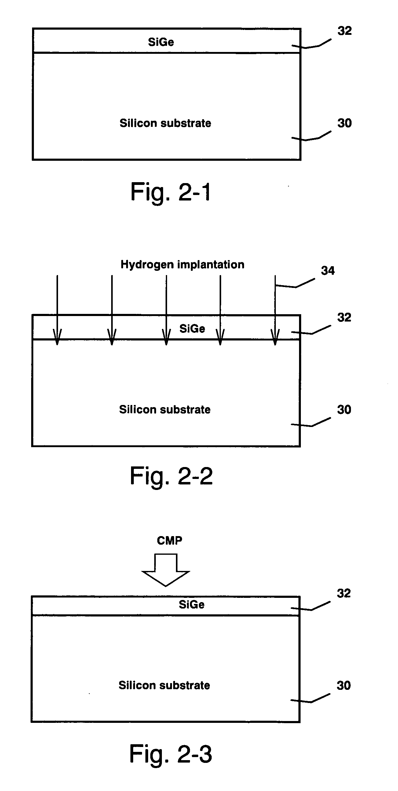
[0036] the present invention SSOI fabrication process employs the fabrication process of a thin relaxed SiGe seed layer and comprises the steps of: [0037] preparing a silicon substrate [0038] preparing a thin relaxed SiGe seed layer by ion implantation [0039] depositing a SiGe layer overlying the silicon substrate [0040] implanting ions into the SiGe layer [0041] annealing to convert the SiGe layer to a relaxed SiGe layer [0042] Polishing the SiGe layer surface and performing a post polishing clean [0043] depositing an epitaxial silicon layer on the relaxed SiGe layer, thereby generating a strained silicon layer [0044] transferring the epitaxial silicon / SiGe multilayer to an insulator layer [0045] implanting ions into the epitaxial silicon / SiGe multilayer to generate a defect zone under the epitaxial silicon / SiGe interface [0046] bonding the epitaxial silicon layer surface of silicon substrate to an insulator layer on a second substrate to form a bonded composite substrate [0047] th...

second embodiment

[0056] the present invention SSOI fabrication process employs the fabrication process of deep split implantation and comprises the steps of: [0057] preparing a silicon substrate [0058] preparing a relaxed SiGe seed layer overlying the silicon substrate whereby a silicon / SiGe interface is formed [0059] depositing an epitaxial silicon layer on the relaxed SiGe layer, thereby generating a strained silicon layer [0060] implanting ions into the epitaxial silicon / SiGe multilayer to generate a defect zone below the substrate silicon / SiGe interface wherein the projected range of the implanted ions is about 100 to 500 nm into the silicon substrate [0061] transferring the epitaxial silicon / SiGe multilayer to an insulator layer [0062] bonding the epitaxial silicon layer surface of silicon substrate to an insulator layer on a second substrate to form a bonded composite substrate [0063] thermally annealing the composite substrate to split the epitaxial silicon / SiGe multilayer along the defect zo...

third embodiment

[0077] the present invention SSOI fabrication process employs the two step annealing process and comprises the steps of: [0078] preparing a silicon substrate [0079] preparing a relaxed SiGe seed layer overlying the silicon substrate whereby a silicon / SiGe interface is formed [0080] depositing an epitaxial silicon layer on the relaxed SiGe layer, thereby generating a strained silicon layer [0081] implanting ions into the epitaxial silicon / SiGe multilayer to generate a defect zone under the epitaxial silicon / SiGe interface [0082] bonding the epitaxial silicon layer surface of silicon substrate to an insulator layer on a second substrate to form a bonded composite substrate [0083] thermally annealing the composite substrate to split the epitaxial silicon / SiGe multilayer along the defect zone at temperature below 400° C. [0084] dry etching to remove part of the silicon substrate and part of the SiGe layer [0085] thermally annealing the composite substrate to improve the bonding at tempe...


PUM


Abstract

Transistors fabricated on SSOI (Strained Silicon On Insulator) substrate, which comprises a strained silicon layer disposed directly on an insulator layer, have enhanced device performance due to the strain-induced band modification of the strained silicon device channel and the limited silicon volume because of the insulator layer. The present invention discloses a SSOI substrate fabrication process comprising various novel approaches. One is the use of a thin relaxed SiGe layer as the strain-induced seed layer to facilitate integration and reduce processing cost. Another is the formation of split implant microcracks deep in the silicon substrate to reduce the number of threading dislocations reaching the strained silicon layer. And lastly is the two step annealing / thinning process for the strained silicon / SiGe multilayer film transfer without blister or flaking formation.

Description

FIELD OF THE INVENTION [0001] This invention relates to integrated circuit (IC) structures and processes, and specifically to an efficient fabrication method of a strained silicon layer on an insulator, yielding a strained silicon-on-insulator (SSOI) structure that is useful for high speed device fabrication. BACKGROUND OF THE INVENTION [0002] Transistors fabricated on Silicon-On-Insulator (SOI) substrate have significant advantages such as higher speed, lower power and higher density than on bulk silicon wafer substrate. The SOI substrate typically consists of a thin surface layer of single crystal silicon on an insulator layer on a bulk silicon wafer. The thin surface silicon layer is the silicon channel of the transistor, and the insulator layer, usually made of silicon dioxide, is commonly referred to as the buried oxide. [0003] SOI wafers improve the transistor performance by reducing the operating silicon volume and by isolating the transistors. The thin surface silicon layer ...

Claims


Application Information

Patent Timeline
Patent Type & Authority Applications(United States)
IPC IPC(8): H01L21/02H01L21/30H01L21/762H01L21/46H01L27/12
CPCH01L21/76254H01L21/76256
Inventor MAA, JER-SHENLEE, JONG-JANTWEET, DOUGLAS J.EVANS, DAVID R.BURMASTER, ALLEN W.HSU, SHENG TENG
Owner SHARP KK
Why Eureka
Try Eureka