Dry etching method and photonic crystal device fabricated by use of the same

a technology of photonic crystal and etching method, which is applied in the field of dry etching method, can solve the problems of low precision, high precision and low roughness, and the inability of the etching method combined with the sidewall protection scheme to manufacture devices which require a large aspect ratio, high precision and low roughness, and achieves the effect of reducing surface roughness

a technology of photonic crystal and etching method, which is applied in the field of dry etching method, can solve the problems of low precision, high precision and low roughness, and the inability of the etching method combined with the sidewall protection scheme to manufacture devices which require a large aspect ratio, high precision and low roughness, and achieves the effect of reducing surface roughness

US20050155951A1Inactive Publication Date: 2005-07-21JAPAN AVIATION ELECTRONICS IND LTD

Image

  • Dry etching method and photonic crystal device fabricated by use of the same
  • Dry etching method and photonic crystal device fabricated by use of the same
  • Dry etching method and photonic crystal device fabricated by use of the same

Examples


embodiment 1

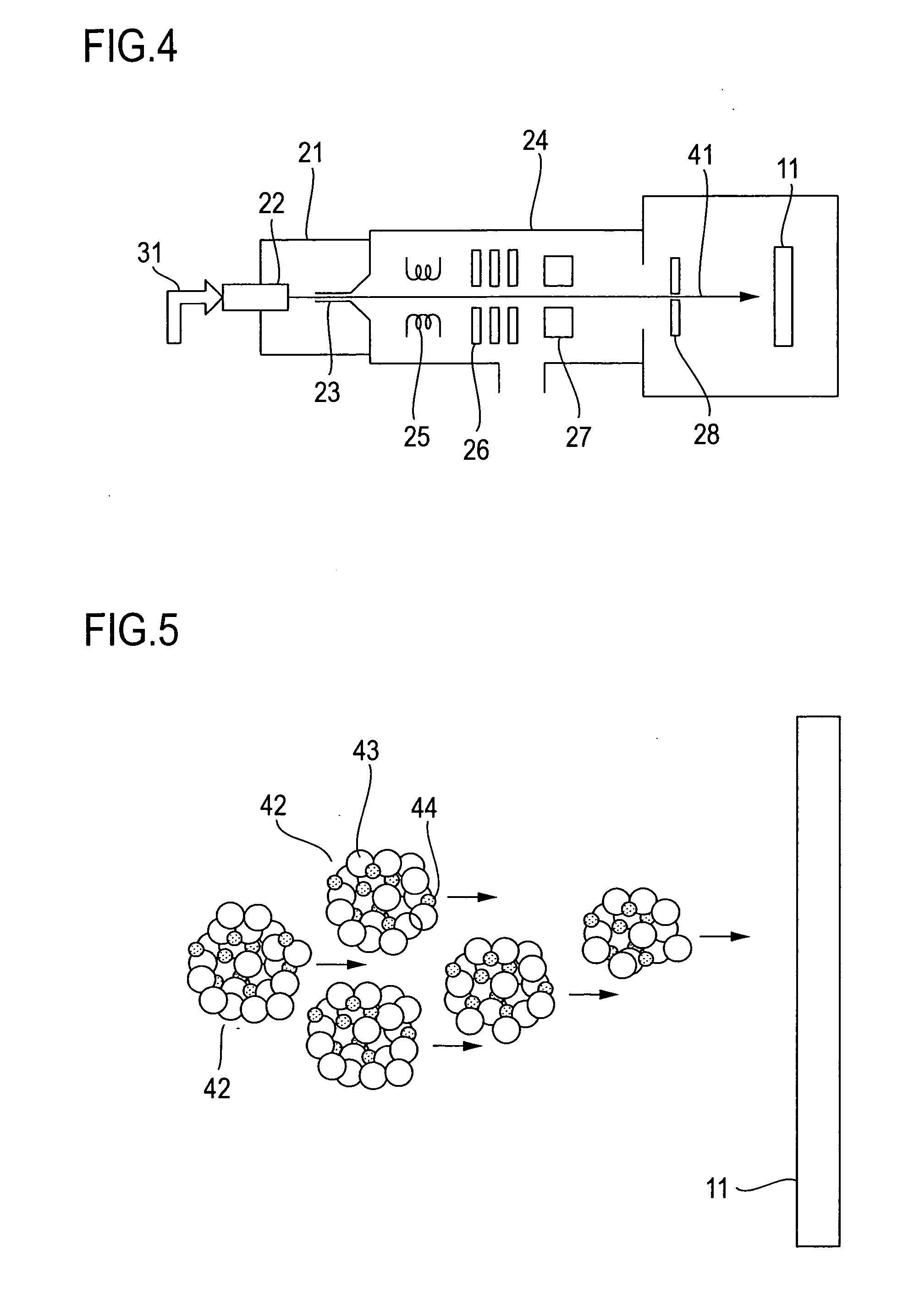
[0051] This embodiment used the cluster ion beam etching device shown in FIG. 4, and used argon (Ar) as an etching gas and a CHF3 gas as a component that reacts with an object surface to deposit and form a thin film. The Ar gas and the CHF3 gas were mixed in a flow rate (mole ratio) of 9:1, then the mixed gas was introduced into the cluster forming chamber 21, from which it was injected via the nozzle 22 to obtain mixed clusters 42. The material of the substrate 11 subject to etching was silicon (Si). The silicon substrate 11 was irradiated with the mixed cluster ion under the condition of a 30 kV acceleration voltage. On the silicon substrate 11 there was preformed a line-and-space pattern by a nickel (Ni) mask. The silicon substrate 11 was irradiated with the cluster ion beam 41 until the depth of etching reached 10 μm.

[0052] For the evaluation of the etching profile, the verticality of the sidewall was evaluated using a scanning electron microscope (SEM) and the sidewall roughne...

embodiment 2

[0053] This embodiment was implemented under basically the same conditions as in Embodiment 1 except changing the acceleration voltage for the mixed cluster ion beam. The acceleration voltage was varied from 0.5 kV to 200 kV. The surface roughness of the sidewall 15 was evaluated using AFM. The results of evaluation are shown in FIG. 8.

embodiment 3

[0054] This embodiment was implemented under basically the same conditions as in Embodiment 1 except changing the flow rate between the Ar gas and th CHF3 gas. The flow rate, Ar / CHF3, was varied from 0.1 to 100. The surface roughness of the sidewall 15 was evaluated using AFM. The results of evaluation are shown in FIG. 9.


PUM

PropertyMeasurementUnit
Acceleration voltageaaaaaaaaaa
Transparencyaaaaaaaaaa
Volatilityaaaaaaaaaa

Abstract

In a dry etching method in which clusters formed by agglomeration of atoms or molecules are ionized and accelerated as a cluster ion beam for irradiation of an object surface to etch away therefrom its constituent atoms, the clusters are mixed clusters 42 formed by agglomeration of two or more kinds of atoms or molecules, and the mixed clusters 42 contain atoms 43 of at least one of argon, neon, xenon and krypton, and a component 44 that is deposited on the object surface to form a thin film by reaction therewith. With this method, it is possible to provide an extremely reduced sidewall surface roughness and high vertical machining accuracy.

Description

BACKGROUND OF THE INVENTION [0001] The present invention relates to a dry etching method for use in the field of microfabrication and, more particularly, to a dry etching method for high-precision microfabrication of a miniature structure of the submicron order with a high aspect ratio and with low surface roughness. The invention also pertains to a photonic crystal device fabricated by use of such a dry etching method. [0002] In the field of microfabrication for integrated circuits and MEMS (Micro-Electro-Mechanical-System) devices there is a growing need for the technique to microfabricate a structure of the submicron order with a high aspect ratio. Furthermore, it is pointed out in the art that the surface roughness of the microfabricated device structure, for example, the surface roughness of its bottom and sidewalls determines the device performance; hence, there is an earnest desire for reduction of the surface roughness. At present, it is customary in the art to fabricate suc...

Claims


Application Information

Patent Timeline
21 Jul 2005
Publication
US20050155951A1
IPC
H01L21/302; B44C1/22; G02B6/122; G02B6/136; H01L21/3065
CPC
B81C1/00531; B81C1/00619; B82Y20/00; H01L21/3065; G02B6/136; H01J2237/0812; G02B6/1225
Inventors
SUZUKI, AKIKO; SATO, AKINOBU