Light-emitting device

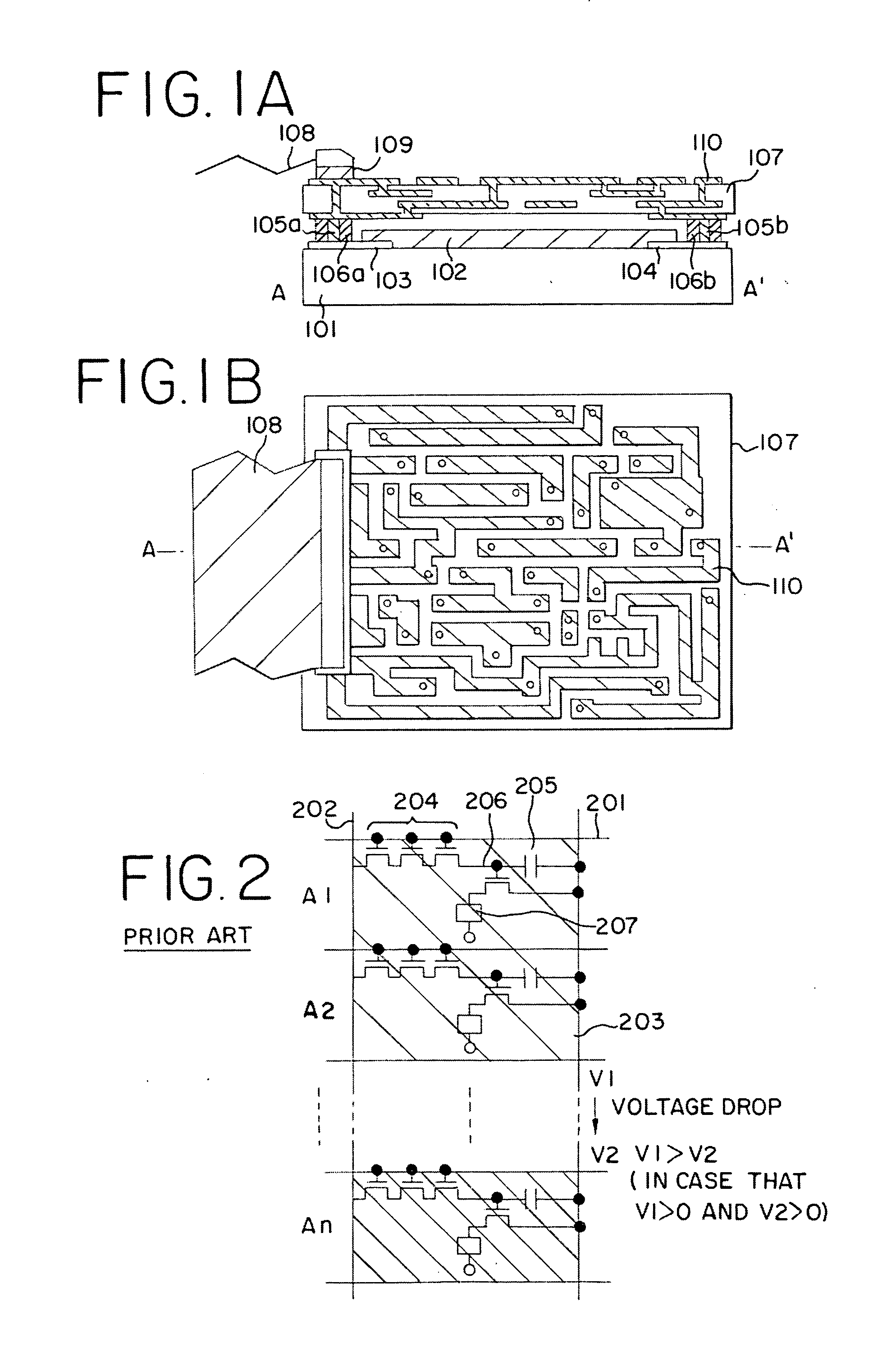
a technology of light-emitting devices and circuits, applied in the direction of organic semiconductor devices, discharge tubes/lamp details, final product manufacturing, etc., can solve the problems of voltage drop, particularly conspicuous problems, wiring resistance, etc., and achieve the effect of enhancing the operating speed of the driver circuit portion and suppressing the delay of wiring

Inactive Publication Date: 2005-07-21
SEMICON ENERGY LAB CO LTD
View PDF22 Cites 22 Cited by
  • Summary
  • Abstract
  • Description
  • Claims
  • Application Information

AI Technical Summary

Benefits of technology

[0016] The present invention has been made in view of the above, and therefore has an object to provide a light-emitting device that has a homogenized quality of image by suppressing an influence of a voltage drop which originates in the above-mentioned wiring resistance. Further, another object of the present invention is to suppress a delay of a wiring which electrically connects a driver circuit portion and an input / output terminal to thereby enhance the operating speed of the driver circuit portion.
[0017] The light-emitting device of the present invention is constituted of a substrate having a luminous element formed thereon (hereinafter referred to as element-formed substrate or a first substrate) and a hardened large printed wiring board (PWB: Printed Wiring Board), which are electrically connected by a conductor (anisotropic conductive film or a bump), and is characterized in that the resistance of each of the wirings (first group of wirings) formed on the element-formed substrate is reduced.

Problems solved by technology

However, in the EL display device which has the current drive, there is a problem of a phenomenon in which a voltage drop (also referred to as an IR drop) caused by a wiring resistance occurs.
This problem is particularly conspicuous when the wiring becomes long.
Thus, it is a large obstacle in making the screen of the EL display device larger.
When the wiring is made of a material such as tantalum, tungsten, or silicon, the EL display device is susceptible to the influence of the wiring resistance, which may become the cause of immensely reducing the homogeneity of the quality of the image.
In addition, the source wiring 202 becomes incapable of applying a desired voltage to a gate of the current control TFT 206 due to the voltage drop, leading to a fear that the brightness of the EL element will change or that the EL element will not emit light.
Thus, the transmission of a desired voltage becomes impossible because of the voltage drop which originates in the wiring resistance.
Consequently, a drawback in which there is a considerable loss in the homogeneity of the quality of the image in the pixel portion occurs.
However, because the wiring is drawn around longer, as a result, the influence of the voltage drop cannot be ignored.
In case of manufacturing a monolithic type light-emitting device in which a driver circuit portion (typically including a gate driver circuit and a source driver circuit) is integrated on the same substrate, the wiring resistance of a wiring that is drawn around between the driver circuit portion and an input terminal of an electric signal becomes a problem.
The wiring resistance induces a delay of the electric signal, and therefore there is a concern that the operating speed of the gate driver circuit and the source driver circuit will be reduced.
Thus, drawbacks such as the considerable loss of the homogeneity of the quality of the image and the extreme decline in the operating speed of the driver circuit portion due to the voltage drop which originates in the wiring resistance and the delay of a signal occur.
Such a problem becomes a particularly conspicuous problem in a light-emitting device having a large screen that is several tens inches in diagonal.

Method used


Image

  • Light-emitting device
  • Light-emitting device
  • Light-emitting device

Examples


embodiment 1

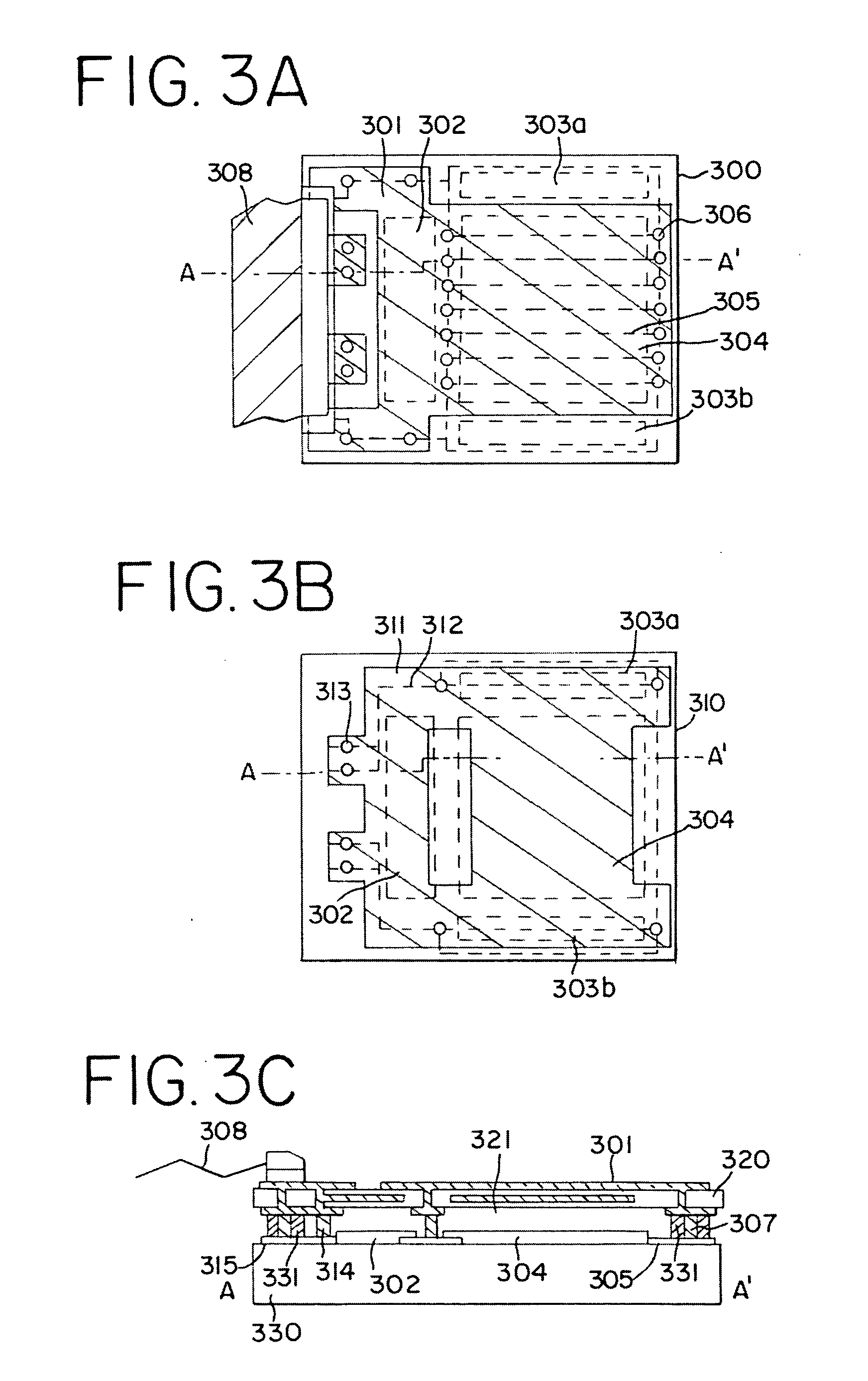
[0052] In Embodiment 1, an explanation will be made with reference to FIGS. 4A and 4B on an active matrix EL display device that is manufactured by employing the present invention. FIG. 4A is a top view of an element-formed substrate (denoted by reference symbol 400 in FIG. 4B) having an EL element formed thereon. Indicated by the dotted lines, reference symbol 401 denotes a source driver circuit, 402 denotes a gate driver circuit, and 403 denotes a pixel portion.

[0053] Further, reference symbol 404 denotes a printed wiring board, and a PWB side wiring 405 is formed thereon. The dotted line indicated by reference symbol 406 denotes a first sealing member, and in the inner side surrounded by the first sealing member 406, resin (denoted by reference symbol 407 in FIG. 4B) is provided between the printed wiring board 404 and the element-formed substrate 400.

[0054] It is to be noted that barium oxide (denoted by reference symbol 408 in FIG. 4B) is used as the moisture absorbent materi...

embodiment 2

[0065] In Embodiment 2, an explanation will be made with reference to FIGS. 5A and 5B on a passive matrix EL display device that is manufactured by employing the present invention. It is to be noted that FIG. 5A is a top view thereof and FIG. 5B is a cross-sectional view thereof taken along the line A-A of FIG. 5A.

[0066] In FIG. 5B, reference symbol 501 denotes an element-formed substrate made of plastic, and reference symbol 502 denotes an a node made of a compound of indium oxide and zinc oxide. In Embodiment 2, the anode 502 is formed by the evaporation method. Though not shown in FIGS. 5A and 5B, it is to be noted that a plurality of anodes are arranged in stripe shapes in a parallel direction in a defined space.

[0067] An insulating film 503 is formed such that it is orthogonal to the plurality of anodes 502 arranged in stripe shapes. In addition, the insulating film 503 is also provided in the gaps of the anodes 502 in order to insulate each of the anodes 502 separately. Ther...

embodiment 3

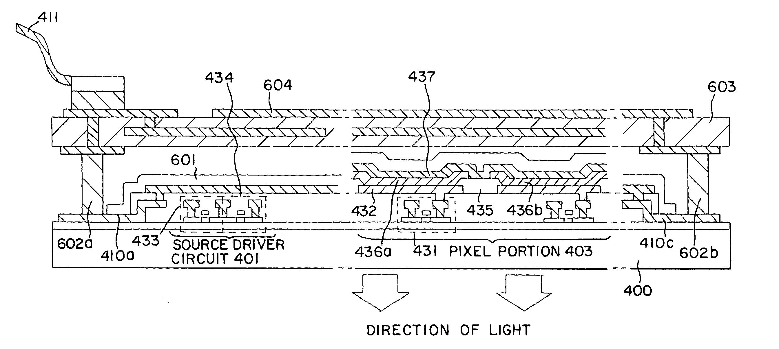
[0081] Shown in Embodiment 3 is a modified example of the structure of the EL display device described in Embodiment 1. The description thereof will be made with reference to FIG. 6. Structures of a TFT and an EL element formed on the element-formed substrate 400 are the same as those of FIGS. 4A and 4B. Therefore, only different components will be denoted with reference symbols and explained.

[0082] Upon forming a structure similar to that of Embodiment 1 up to the formation of the cathode 437, a passivation film 601 is further formed to a thickness of 50 to 500 nm (preferably between 300 and 400 nm) to cover the cathode 437. As the passivation film 601, a tantalum oxide film, a silicon nitride film, a silicon oxide film, a silicon oxide nitride film, or a lamination film of a combination thereof may be used. It is preferable that the film deposition thereof is performed at a temperature of 150° C. or less by vapor-phase deposition such that the EL element will not deteriorate.

[00...


PUM

PropertyMeasurementUnit
thicknessaaaaaaaaaa
thicknessaaaaaaaaaa
thicknessaaaaaaaaaa

Abstract

A light-emitting device having the quality of an image high in homogeneity is provided. A printed wiring board (second substrate) (107) is provided facing a substrate (first substrate) (101) that has a luminous element (102) formed thereon. A PWB side wiring (second group of wirings) (110) on the printed wiring board (107) is electrically connected to element side wirings (first group of wirings) (103, 104) by anisotropic conductive films (105a, 105b). At this point, because a low resistant copper foil is used to form the PWB side wiring (110), a voltage drop of the element side wirings (103, 104) and a delay of a signal can be reduced. Accordingly, the homogeneity of the quality of an image is improved, and the operating speed of a driver circuit portion is enhanced.

Description

BACKGROUND OF THE INVENTION [0001] 1. Field of the Invention [0002] The present invention relates to a device having an element (hereinafter referred to as luminous element) that is comprised of a luminous material sandwiched between electrodes (the device will hereinafter be referred to as light-emitting device), and to a method of manufacturing the same. Specifically, the present invention relates to a light-emitting device using a luminous material that provides EL (Electro Luminescence) (hereinafter referred to as EL material). [0003] 2. Description of the Related Art [0004] In recent years, development is proceeding in a light-emitting device (EL display device) using a luminous element that utilizes the EL phenomenon of a luminous material (hereinafter referred to as EL element). The EL display device is a display device that uses a luminous element which itself has a light-emitting ability, that is, self-emissive, and hence, unlike a liquid crystal display device, does not ne...

Claims


Application Information

Patent Timeline
Patent Type & Authority Applications(United States)
IPC IPC(8): H05B33/04G01N33/497G09F9/00G09F9/30H01L27/32H01L31/12H01L51/50H04N5/70H05B33/06H05B33/14H05B44/00
CPCG01N33/497H05K2201/1031H01L27/3279H01L27/3288H01L27/329H01L51/524H01L2251/5315H01L33/62H01L51/5203H01L27/124H01L31/153H01L2924/0002H01L27/3276H05K2201/093H05K2201/10128H05K3/323H05K3/361H05K1/0298H01L2924/00Y02E10/549Y02P70/50H10K59/1795H10K59/179H10K59/1315H10K59/131H10K2102/3026H10K59/871H01L31/12H10K50/841H10K50/805H10K59/60H10K59/1213H10K71/00H10K77/111H10K59/1201H10K2102/311H01L27/1218
Inventor YAMAZAKI, SHUNPEIFUKUNAGA, TAKESHI
Owner SEMICON ENERGY LAB CO LTD
Why Eureka
Try Eureka