A/D conversion device having input level shift and output correction function

a conversion device and input level technology, applied in the field of a/d conversion devices, can solve the problems of a/d conversion error, add the cost of the filter circuit b>7/b> that is an external part,

Inactive Publication Date: 2005-08-04
DENSO CORP
View PDF2 Cites 6 Cited by
  • Summary
  • Abstract
  • Description
  • Claims
  • Application Information

AI Technical Summary

Benefits of technology

[0020] Preferably, in the input voltage range handled by the first level shift circuit, the correction is performed at two points, that is, the maximum value and the center value of the input voltage range of the A / D converter. In the input voltage range handled by the second level shift circuit, the correction is performed at two points, that is, the center value and the minimum value of the input voltage range of the A / D converter. As a result, it becomes possible to correct the shift characteristic of the level shift circuit, and to correct the nonlinearity of the A / D converter, as described above.

Problems solved by technology

As a result, the input voltage of the channel selected last time remains in the parasitic capacitor Cf, and an A / D conversion error arises due to its effect.
As a result, a current flows from the input terminal 2 of the selected channel into the parasitic capacitor Cf, which is now at the ground potential, producing an error arising from delay in stabilizing the voltage of the common line 3.
In addition, the necessity of setting the electrostatic capacity of the capacitor C1 constituting the filter circuit 7 to a large value will add cost of the filter circuit 7 that is an external part.

Method used


Image

  • A/D conversion device having input level shift and output correction function
  • A/D conversion device having input level shift and output correction function
  • A/D conversion device having input level shift and output correction function

Examples


first embodiment

[0032] A first embodiment of an A / D conversion device in a single channel configuration will be described referring to FIGS. 1 to 5.

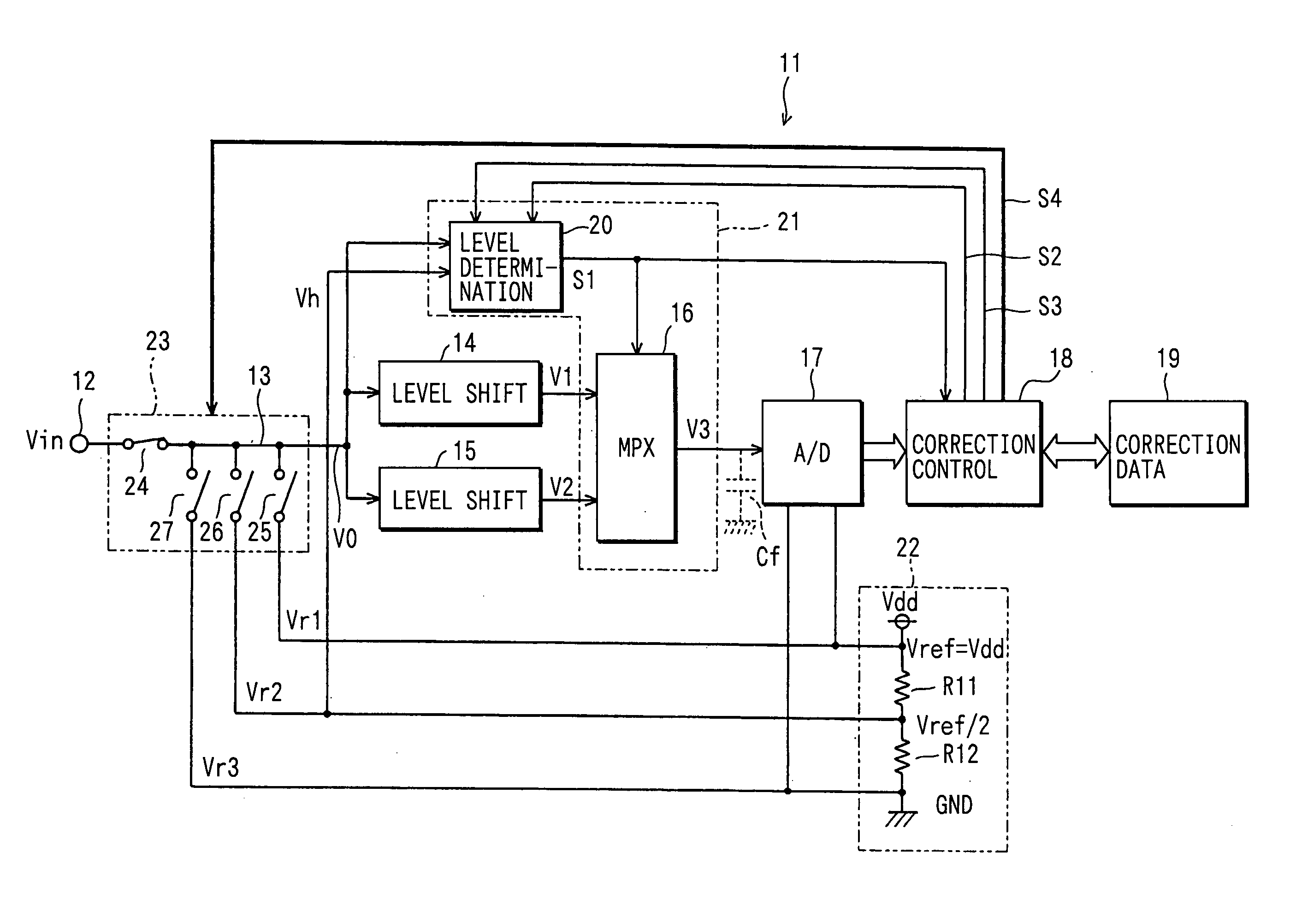
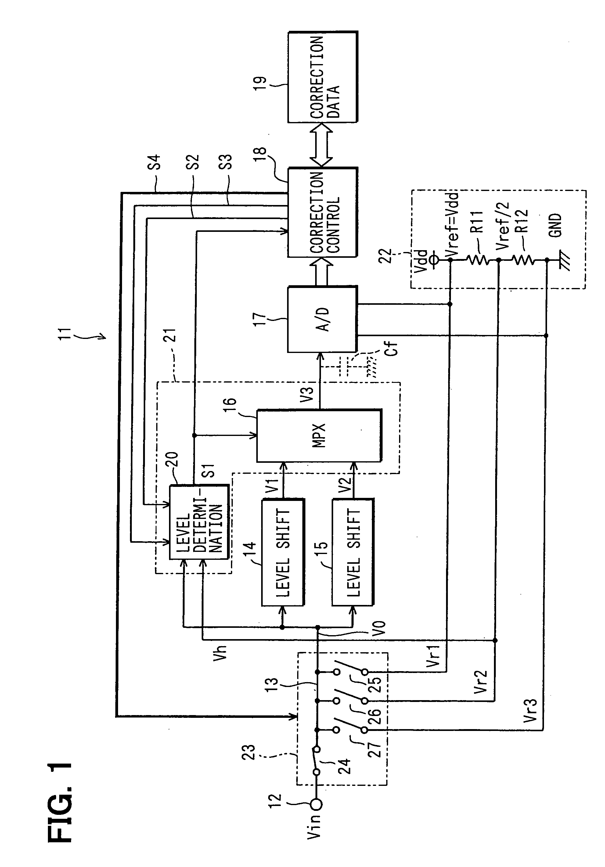
[0033] As shown in FIG. 1, an A / D conversion device 11 is constructed as an IC (semiconductor integrated circuit device) that uses the MOS semiconductor manufacture process, and is incorporated as a peripheral of, for example, a one-chip microcomputer. The A / D conversion device 11 has a normal mode, in which a signal voltage Vin inputted from the outside of the IC is A / D converted. It also has a correction mode, in which predetermined reference voltages Vr1, Vr2 and Vr3 are A / D converted to acquire correction values serving as correction references (correction data).

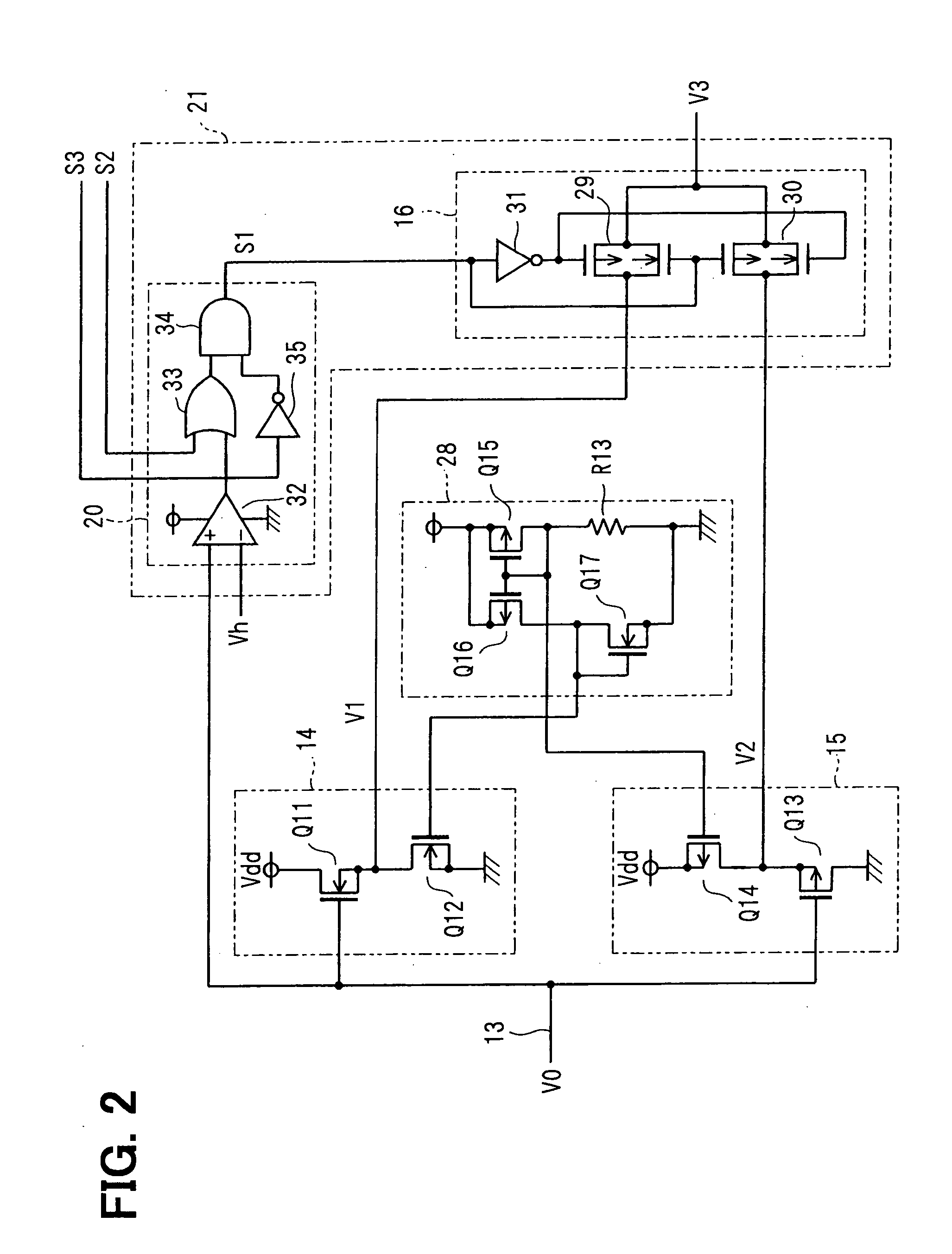
[0034] An input terminal 12 through which a signal voltage Vin is inputted from the outside of the IC is connected to two level shift circuits 14, 15 through an input line 13. The level shift circuit 14 shifts an input voltage V0 given to the input line 13 (the signal voltage Vin or the re...

second embodiment

[0074]FIG. 6 shows an A / D conversion device 36 according to the second embodiment. This A / D conversion device 36 differs from the A / D conversion device 11 shown in FIG. 1 in the configuration of level shift circuits 37, 38. In this embodiment, the acquisition of the correction values using the reference voltage Vr2 (=Vref / 2) becomes unnecessary in the correction mode. Accordingly, an input switching circuit 39 is not equipped with the switching circuit 26 of the first embodiment.

[0075]FIG. 7 shows a circuit configuration of the level shift circuits 37, 38. The gate and the drain of the level shift circuit 37 are coupled through an operational amplifier 40 having a connection mode of a voltage follower. The gate and the drain of the level shift circuit 38 are coupled through an operational amplifier 41 having a connection mode of a voltage follower. The rest of the configuration is the same as that of the level shift circuits 14, 15 of the first embodiment.

[0076] According to this ...

third embodiment

[0078] An A / D converter circuit device 42 according to a third embodiment is constructed in a multi-channel configuration as shown in FIG. 8.

[0079] This A / D conversion device 42 is similar to the A / D conversion device 11 of the first embodiment, but the number of channels is increased to eight. Each of channel 0 through channel 7 needs the input terminal 12, the input switching circuit 23, and the level shift circuits 14, 15. In the figure, portions surrounded by broken lines are of the same configuration, so the whole configuration is shown therein with channel 1 through channel 7 omitted.

[0080] Between the level shift circuits 14, 15 and the multiplexer 16 of each channel, a multiplexer 43 is provided for selecting output voltages V1, V2 of the level shift circuits 14, 15 of any one of the channels. This multiplexer 43 is so configured that switching thereof is controlled by a control signal S5 outputted from the correction control circuit 18.

[0081] Like the A / D conversion devi...


PUM


Abstract

In an A/D conversion device, one level shift circuit shifts an input voltage to the low potential side by Vt1, and another level shift circuit shifts the input voltage to the high potential side by Vt2. A multiplexer selects either of the shifted voltages to an A/D converter. In a correction mode, a correction data holding circuit holds values of reference voltages that are also A/D converted after being passed through the one level shift circuit and values of reference voltages that are A/D converted by being passed through the other level shift circuit, as correction values. A correction control circuit corrects the A/D converted value using the correction values.

Description

CROSS REFERENCE TO RELATED APPLICATION [0001] This application is based on and incorporates herein by reference Japanese Patent Application No. 2004-23300 filed on Jan. 30, 2004. FIELD OF THE INVENTION [0002] The present invention relates to an A / D conversion device suitable for both single channel configuration and multi-channel configuration. BACKGROUND OF THE INVENTION [0003]FIG. 9 shows one example of a multi-channel A / D conversion device, which is so configured that a voltage of each input terminal 2 is selected by an analog multiplexer 1 and the selected input voltage is given to an A / D converter 4 through a common line 3. A parasitic capacitor Cf generally exists in the analog multiplexer 1 as shown by a broken line in the figure. As a result, the input voltage of the channel selected last time remains in the parasitic capacitor Cf, and an A / D conversion error arises due to its effect. Therefore, the input part of each channel is equipped with a buffer amplifier 5. [0004] In ...

Claims


Application Information

Patent Timeline
Patent Type & Authority Applications(United States)
IPC IPC(8): H03M1/06H03M1/18H03M1/12H03M1/34
CPCH03M1/181
Inventor HARADA, TAKUYA
Owner DENSO CORP
Why Eureka
Try Eureka