Integrated getter area for wafer level encapsulated microelectromechanical systems

a microelectromechanical system and integrated technology, applied in the direction of acceleration measurement using interia forces, instruments, coatings, etc., can solve the problems of increasing instability, and affecting the efficiency of the getter material

Active Publication Date: 2005-08-18
ROBERT BOSCH GMBH
View PDF18 Cites 37 Cited by
  • Summary
  • Abstract
  • Description
  • Claims
  • Application Information

AI Technical Summary

Benefits of technology

[0007] Thus, there is a need for, among other things, a MEMS employing thin film wafer level packaging techniques that overcomes one, some or all of the shortcomings pertaining to gettering and volume constraints of the conventional thin film wafer level packaging techniques. There is a need for, among other things, a MEMS, including mechanical structures that are encapsulated using thin film encapsulation, that includes enhanced getter capabilities and / or an enhanced volume of the chamber containing the mechanical structures with little to no increase in overall dimensions of the MEMS. In this way, the thin film wafer level packaged MEMS of the present invention includes a relatively stable, controlled pressure environment within the chamber to provide, for example, a more stable predetermined, desired and / or selected mechanical damping of the mechanical structure(s). SUMMARY OF THE INVENTION
[0009] In one embodiment, sealing the chamber by depositing the thin film encapsulation structure may include depositing a sacrificial layer around at least a portion of the mechanical structure and the periphery area and depositing a first encapsulation layer over the sacrificial layer. Thereafter, at least one vent may be formed through the first encapsulation layer (for example, polycrystalline silicon, amorphous silicon, germanium, silicon / germanium and / or gallium arsenide) to allow removal of at least a portion of the sacrificial layer. After removing at least a portion of the sacrificial layer from the mechanical structure and the periphery area, a second encapsulation layer (for example, is a semiconductor material which comprises of polycrystalline silicon, amorphous silicon, silicon carbide, silicon / germanium, germanium and / or gallium arsenide) may be deposited over or in the vent to seal the chamber.

Problems solved by technology

In addition, due to subsequent processing (often at high temperatures), thin film wafer level packaged MEMS are not able to effectively employ a getter material to “capture” impurities, atoms and / or molecules that are out-gassed from surrounding materials.
As such, conventional thin film wafer level packaged MEMS are more susceptible to pressure instability within the chamber.
This instability may increase over time and operating conditions (for example, operating over a large range of operating temperatures).

Method used


Image

  • Integrated getter area for wafer level encapsulated microelectromechanical systems
  • Integrated getter area for wafer level encapsulated microelectromechanical systems
  • Integrated getter area for wafer level encapsulated microelectromechanical systems

Examples


Embodiment Construction

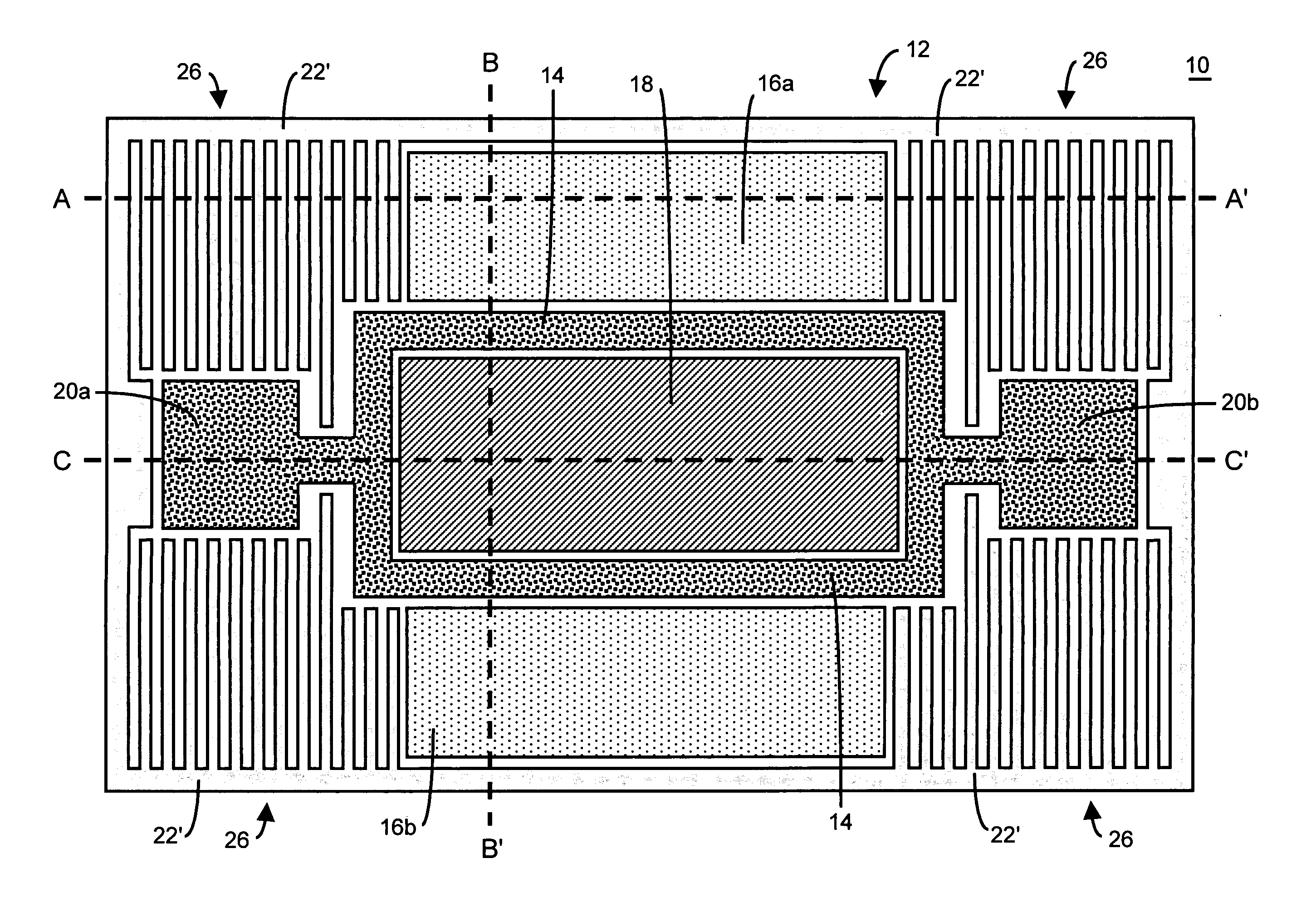
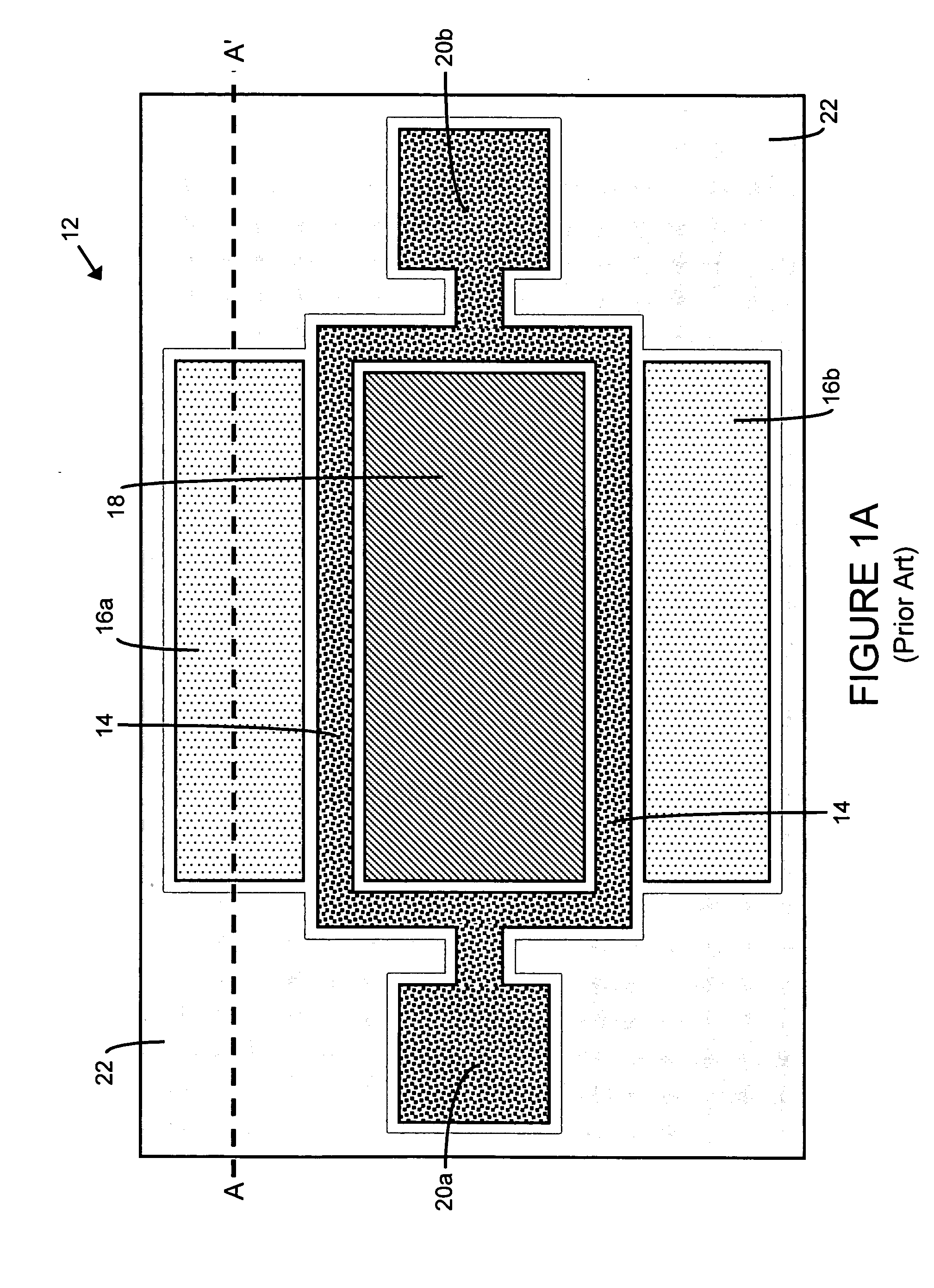
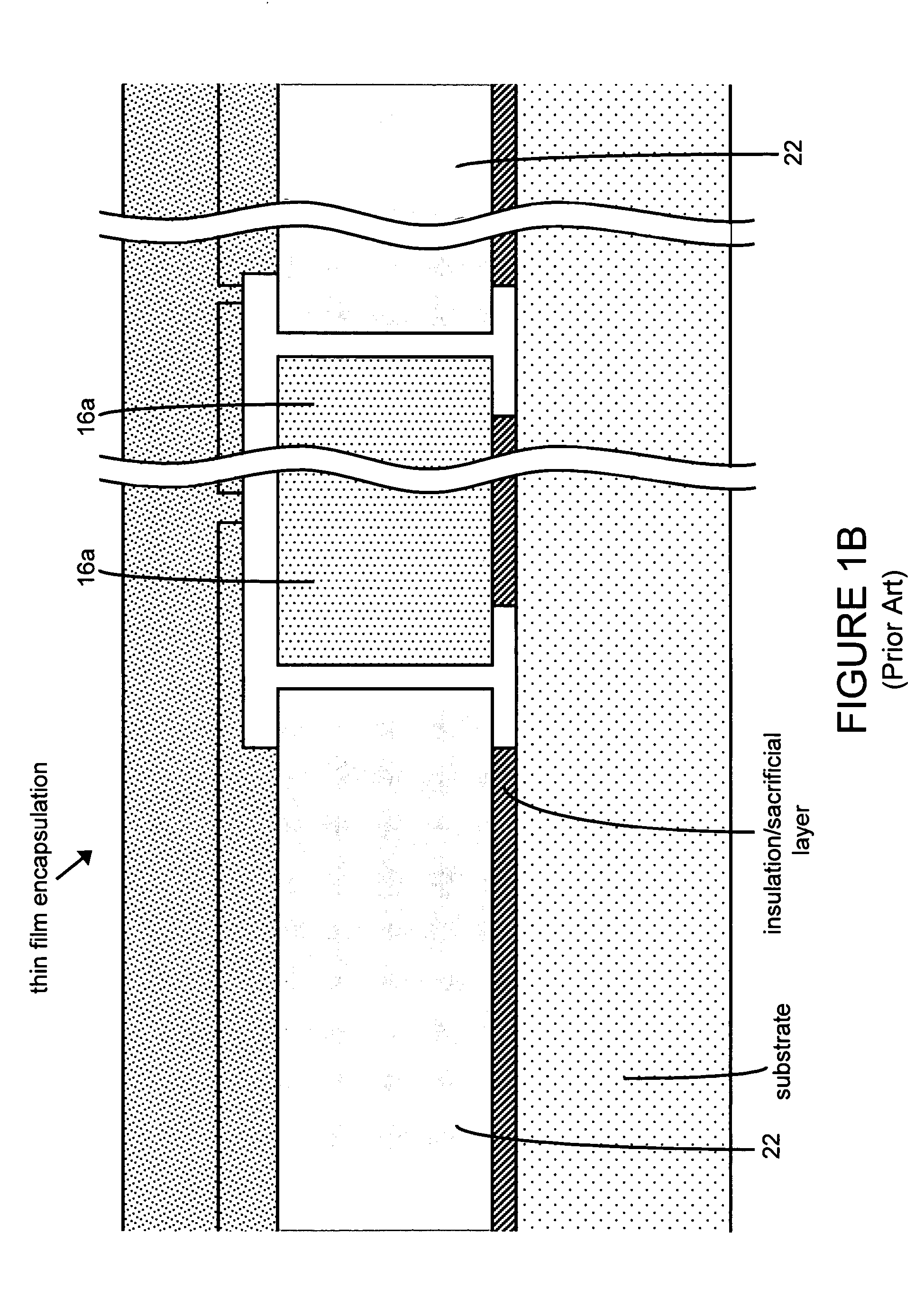
[0036] There are many inventions described and illustrated herein. In one aspect, the present invention is directed to a thin film encapsulated MEMS, and technique of fabricating or manufacturing a thin film encapsulated MEMS, having an integrated getter area and / or an enhanced chamber volume which, from the perspective of the mechanical structure and chamber, causes little to no increase in overall dimension(s) of the MEMS. The integrated getter area is disposed within the chamber and is capable of (i) “capturing” impurities, atoms and / or molecules that are out-gassed from surrounding materials and / or (ii) reducing and / or minimizing the adverse impact of such impurities, atoms and / or molecules (for example, reducing the probability of adding mass to a resonator which would thereby change the resonator's frequency). In this way, the thin film wafer level packaged MEMS of the present invention includes a relatively stable, controlled pressure environment within the chamber to provide...


PUM

PropertyMeasurementUnit
thicknessaaaaaaaaaa
thicknessaaaaaaaaaa
aperture sizeaaaaaaaaaa

Abstract

There are many inventions described and illustrated herein. In one aspect, present invention is directed to a thin film encapsulated MEMS, and technique of fabricating or manufacturing a thin film encapsulated MEMS including an integrated getter area and / or an increased chamber volume, which causes little to no increase in overall dimension(s) from the perspective of the mechanical structure and chamber. The integrated getter area is disposed within the chamber and is capable of (i) “capturing” impurities, atoms and / or molecules that are out-gassed from surrounding materials and / or (ii) reducing and / or minimizing the adverse impact of such impurities, atoms and / or molecules (for example, reducing the probability of adding mass to a resonator which would thereby change the resonator's frequency). In this way, the thin film wafer level packaged MEMS of the present invention includes a relatively stable, controlled pressure environment within the chamber to provide, for example, a more stable predetermined, desired and / or selected mechanical damping of the mechanical structure.

Description

[0001] This invention relates to microelectromechanical systems and / or nanoelectromechanical systems (collectively hereinafter “microelectromechanical systems”) and techniques for fabricating microelectromechanical systems; and more particularly, in one aspect, for fabricating or manufacturing microelectromechanical systems having mechanical structures that are encapsulated using thin film or wafer level encapsulation techniques in a chamber, and including an integrated getter area and / or an enhanced volume of the chamber. [0002] Microelectromechanical systems (“MEMS”), for example, gyroscopes, resonators and accelerometers, utilize micromachining techniques (i.e., lithographic and other precision fabrication techniques) to reduce mechanical components to a scale that is generally comparable to microelectronics. MEMS typically include a mechanical structure fabricated from or on, for example, a silicon substrate using micromachining techniques. For example, with reference to FIG. 1A...

Claims


Application Information

Patent Timeline
Patent Type & Authority Applications(United States)
IPC IPC(8): B81C1/00H01L21/00H01L29/84
CPCB81C1/00269B81C1/00285B81B7/0038H01L2224/48091B81C2203/0136H01L2924/00014
Inventor LUTZ, MARKUSPARTRIDGE, AARON
Owner ROBERT BOSCH GMBH
Why Eureka
Try Eureka