Gate electrode dopant activation method for semiconductor manufacturing
- Summary
- Abstract
- Description
- Claims
- Application Information
AI Technical Summary
Problems solved by technology
Method used
Image
Examples
Embodiment Construction
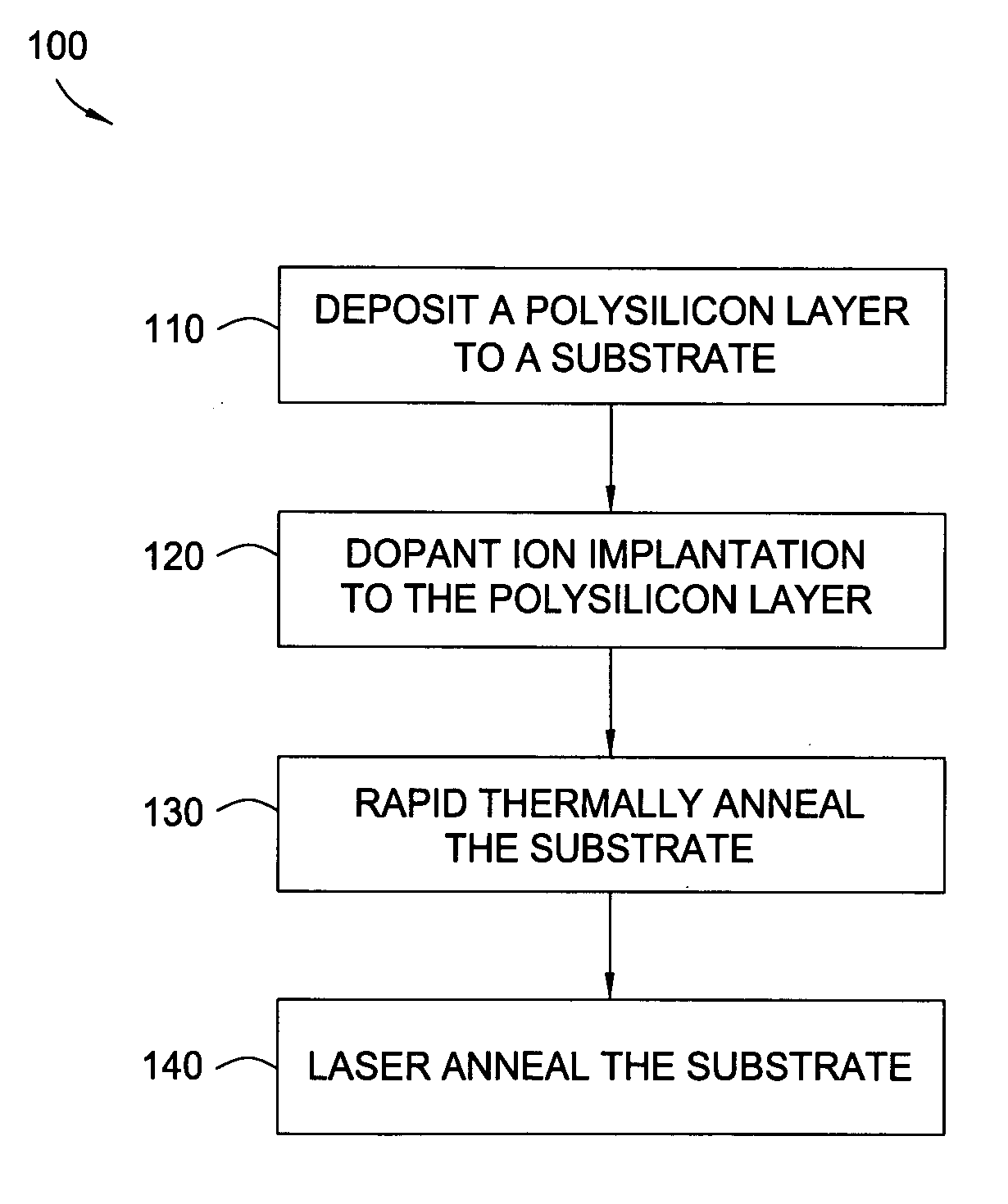
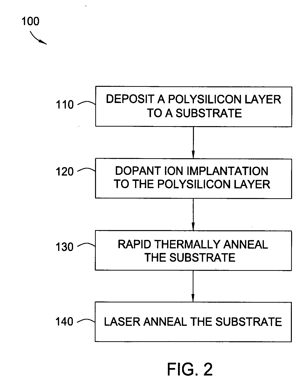
[0017] The present invention teaches methods for forming a doped polycrystalline silicon layer onto a dielectric material, such as silicon dioxide, silicon oxynitride or a high dielectric constant material. Generally, the polycrystalline layer is doped by ion implantation, thermally annealed, such as with a rapid thermal annealing (RTA) process, and subsequently laser annealed to activate the dopants by a dynamic surface anneal (DSA) process.
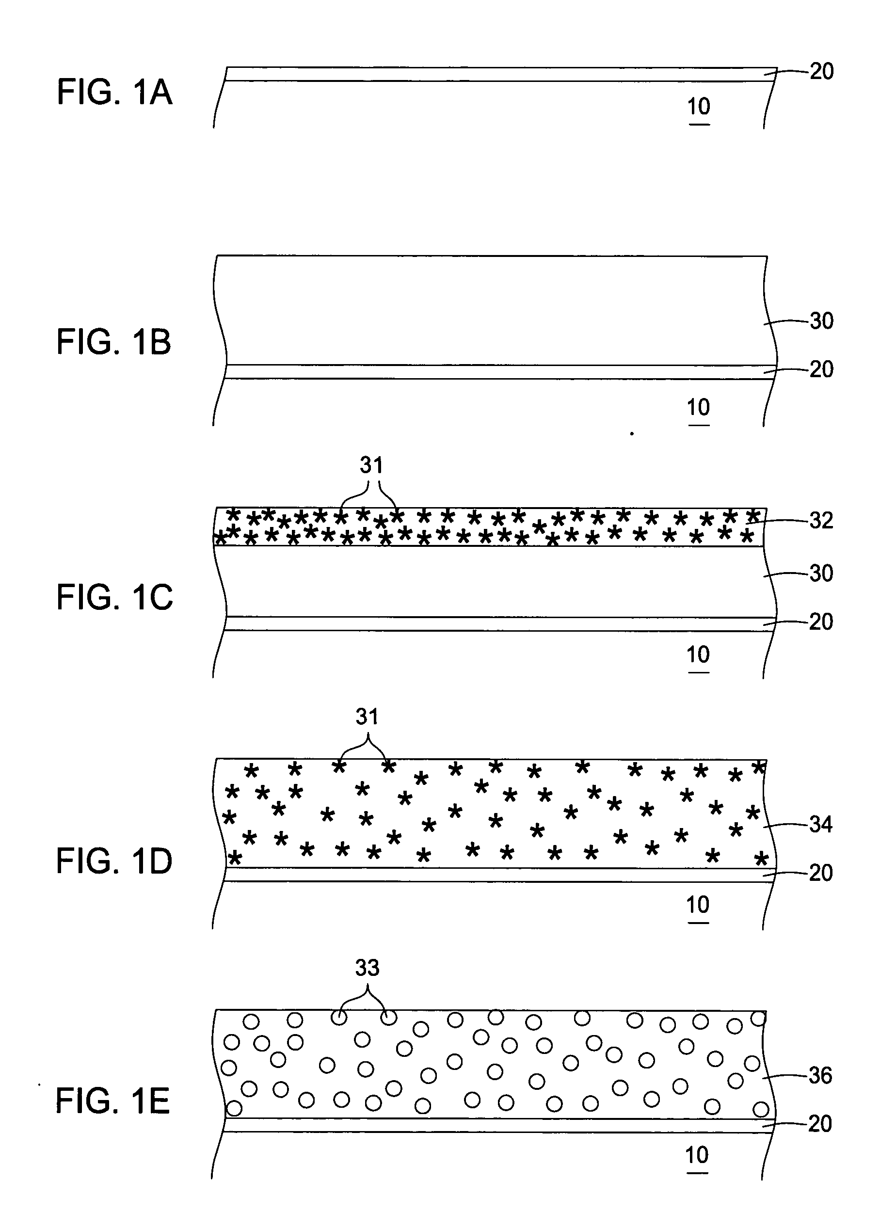
[0018]FIGS. 1A-1E show a cross-sectional view of a gate stack structure progressing through processes disclosed in the present invention. FIG. 1A depicts a dielectric layer 20 disposed on a substrate 10, such as a silicon substrate used in semiconductor processes. In one example, substrate 10 may be a 300 mm p-type silicon substrate doped with boron to resistivity from about 15 Ω-cm to about 20 Ω-cm and is usually pre-cleaned with a conventional pre-gate clean prior to the deposition of dielectric layer 20.
[0019] Dielectric layer 20 may be dep...
PUM
 Abstract
Description
Claims
Application Information


