Laser irradiation apparatus laser irradiation method, semiconductor device and method of manufacturing a semiconductor device

a laser irradiation and laser irradiation technology, applied in laser beam welding apparatus, manufacturing tools, solid-state devices, etc., can solve the problems of substantial damage to the characteristics of semiconductor devices, the average grain size of the obtained polycrystalline silicon film cannot be larger than 500 nm, and the grain size cannot be markedly larger by any method, so as to reduce the concentration of hydrogen and improve the film characteristic to withstand laser energy

Inactive Publication Date: 2005-08-09
SEMICON ENERGY LAB CO LTD
View PDF53 Cites 57 Cited by
  • Summary
  • Abstract
  • Description
  • Claims
  • Application Information

AI Technical Summary

Benefits of technology

[0014]An object of the present invention is to solve the above problem by providing a laser irradiation apparatus and a laser irradiation method to thereby grow 500 nm or larger, preferably 1 μm or greater, crystal grains.
[0022]The substrate is then exposed in an atmosphere containing nitrogen gas at 500° C. for 1 hour to thereby reduce the concentration of hydrogen in the amorphous silicon film. This process has considerably improved the film characteristic to withstand laser energy.

Problems solved by technology

A large number of lattice defects exist in the grain boundary of these crystal grains causing substantial damages to the characteristics of a semiconductor device.
However, the average grain size of the polycrystalline silicon film obtained could not be larger than 500 nm.
In any case, the grain size could not be made markedly bigger by any of the methods.

Method used


Image

  • Laser irradiation apparatus laser irradiation method, semiconductor device and method of manufacturing a semiconductor device
  • Laser irradiation apparatus laser irradiation method, semiconductor device and method of manufacturing a semiconductor device
  • Laser irradiation apparatus laser irradiation method, semiconductor device and method of manufacturing a semiconductor device

Examples


embodiment 1

[0089]An example of laser annealing an amorphous silicon film is shown here in Embodiment 1.

[0090]A 0.7 mm thick Corning 1737 is used as a substrate. This substrate has sufficient durability up to a temperature of 600° C. A 200 nm SiO2 film is deposited on one surface of the substrate. In addition, a 55 nm a-Si film is deposited on top. Plasma CVD is used for both film depositions. Other means of film deposition; such as sputtering, can be employed.

[0091]The substrate, on which the above films have been deposited, is exposed in a nitrogen atmosphere at 500° C. for 1 hour. This process is one for reducing the concentration of hydrogen in the a-Si film. Accordingly, the characteristic of the a-Si film to withstand laser can be raised immensely. A hydrogen concentration on the order of 1020 atoms / cm3 in the film is suitable.

[0092]Next, the substrate 703 is placed in a chamber 707 as shown in FIG. 6. The substrate is arranged in a direction parallel to gravity and fixed in place by fast...

embodiment 2

[0124]An example of a polycrystalline silicon film irradiated with a laser is shown here in Embodiment 2.

[0125]A 0.7 mm thick Corning 1737 is prepared as a substrate. This substrate has sufficient durability up to a temperature of 600° C. A 200 nm SiO2 film is deposited on one side of the substrate. In addition, a 55 nm thick a-Si film is deposited on top. Plasma CVD is used for both film depositions. Other means of film deposition, such as sputtering, can be employed.

[0126]First, an aqueous nickel acetate solution with a concentration of 10 ppm is applied on the a-Si film, and then exposed to a nitrogen atmosphere at 550° C. for 4 hours, performing crystallization of the amorphous silicon film. Spin coating may be used as the application method. The amorphous silicon film doped with nickel by this technique is crystallized at a low temperature over a short time. It is thought that the cause of this is that the nickel fulfills the role of a crystal growth nucleus, promoting the crys...

embodiment 3

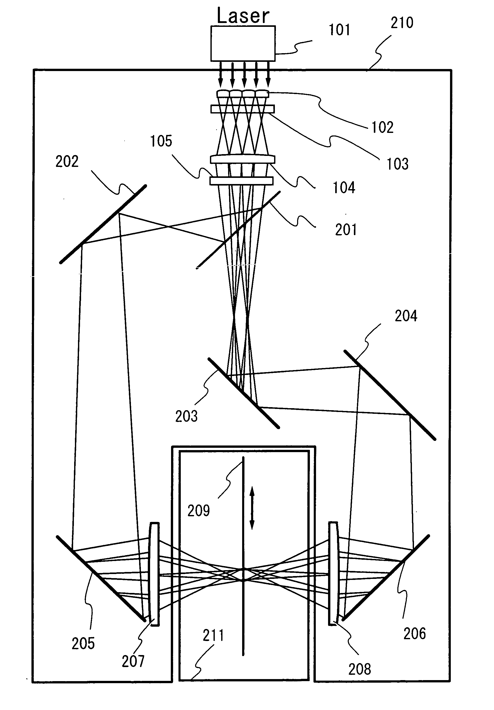
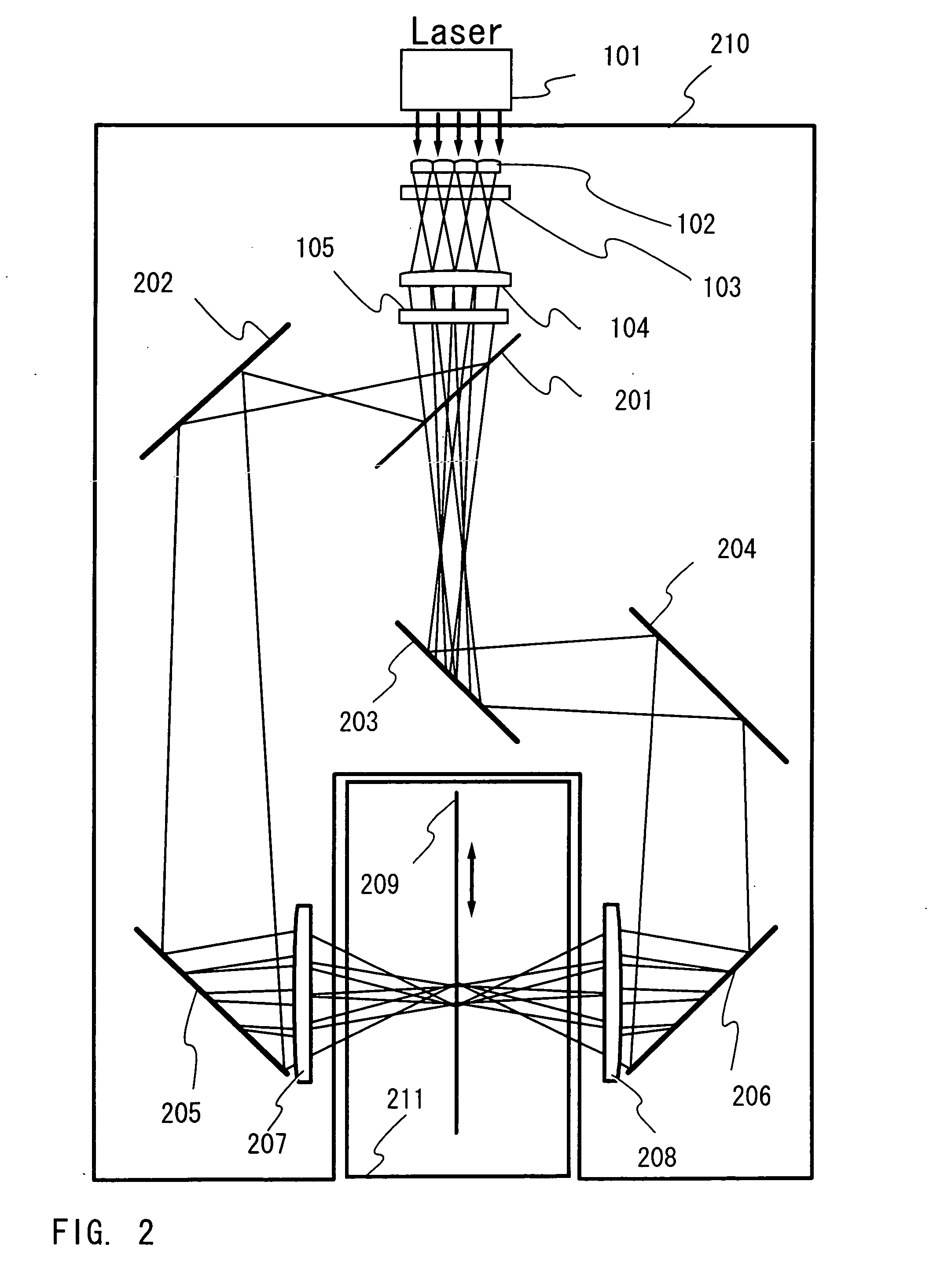
[0128]Embodiment 3 shows an example of employing an optical system different from the optical system indicated in the embodiment modes of the present invention. The modified optical system is explained with reference to FIG. 4.

[0129]The optical system of FIG. 4 is similar to that of FIG. 2 in that a laser is irradiated from the front surface and the back surface of a substrate. The symbols that are the same as those of FIG. 2 denote the same members.

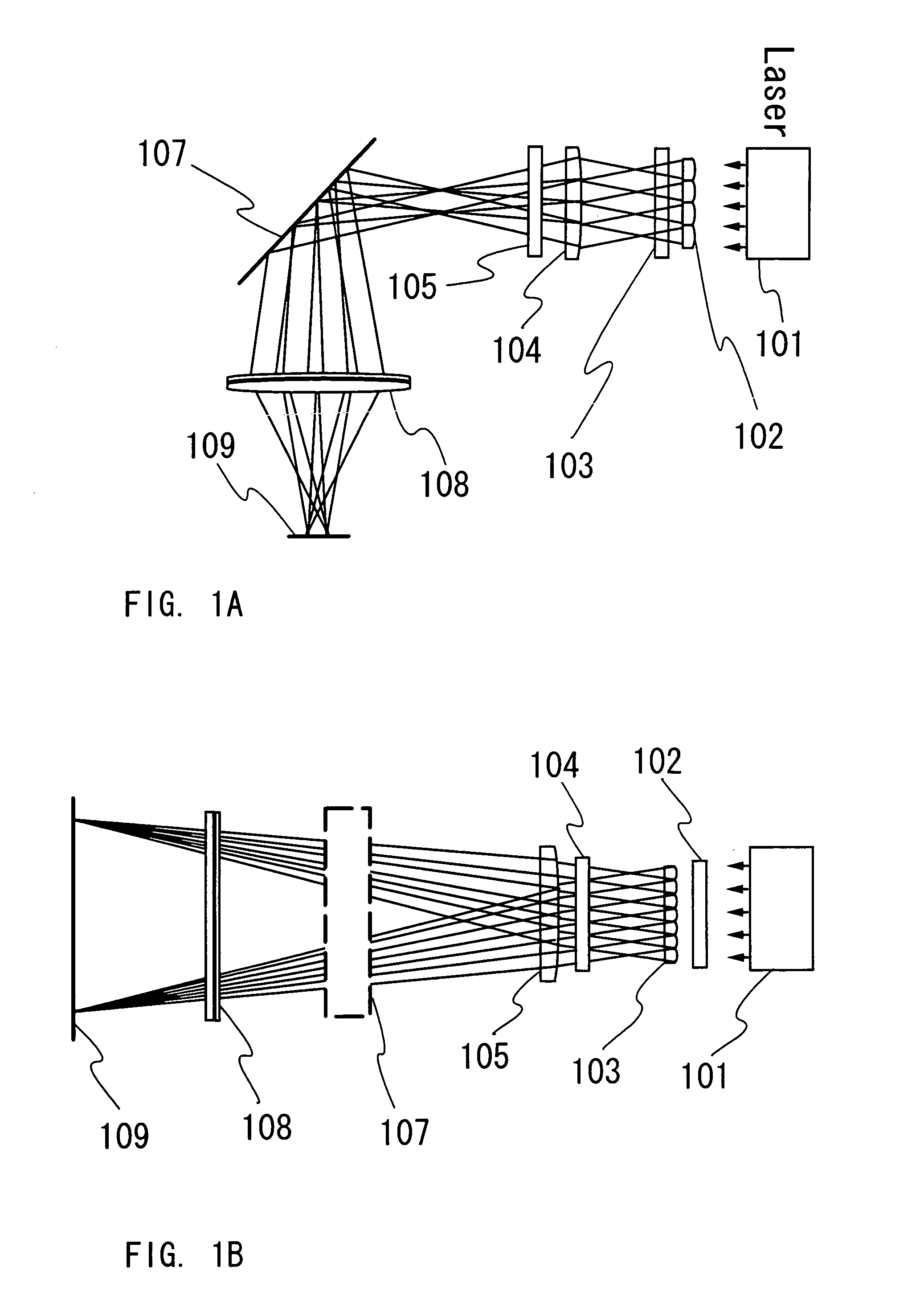
[0130]A laser beam emitted from the laser oscillator 101 is split by the cylindrical lens array 103, and synthesized on the irradiation surface 209 by the cylindrical lens 105. The details of this structure are mentioned in the explanation of FIG. 1. This makes energy in the longitudinal direction of the linear shape laser beam on the irradiation surface uniform and determines its length.

[0131]On the other hand, the uniformity of the energy of the linear shape laser in the width direction is attained by reflection mirrors 501 and 502 hav...


PUM

PropertyMeasurementUnit
atmospheric pressureaaaaaaaaaa
grain sizeaaaaaaaaaa

Abstract

To form a polycrystalline silicon film having a grain size of 1 μm or greater by means of laser annealing. A beam emitted from a laser apparatus (101) is split in two by a half mirror. The split beams are processed into linear shapes by cylindrical lenses (102) to (105), and (207), then simultaneously irradiate an irradiation surface (209). If an amorphous silicon film formed on a glass substrate is disposed on the irradiation surface (209), an area will be irradiated by both a linear shape beam entering from a front surface and a linear shape beam that has transmitted through the glass surface. Both linear shape beams irradiate the same area to thereby crystallize the amorphous silicon film.

Description

BACKGROUND OF THE INVENTION[0001]1. Field of the Invention[0002]The present invention relates to an apparatus for manufacturing a semiconductor device having a circuit comprising thin film transistors. For example, the invention relates to an apparatus for manufacturing an electro-optical device, typically a liquid crystal display device, and the structure of electric equipment mounted with such an electro-optical device as a component. Note that throughout this specification, the semiconductor device indicates general devices that may function by use of semiconductor characteristics, and that the above electro-optical device and electric equipment are categorized as the semiconductor device.[0003]2. Description of the Related Art[0004]In recent years, the technique of crystallizing and improving the crystallinity of an amorphous semiconductor film or a crystalline semiconductor film (a semiconductor film having a crystallinity which is polycrystalline or microcrystalline, but is no...

Claims


Application Information

Patent Timeline
Patent Type & Authority Patents(United States)
IPC IPC(8): B23K26/02H01L21/70H01L21/42H01L21/336H01L21/00H01L21/477H01L21/26H01L21/268H01L21/02H01L21/324H01L21/84B23K26/067H01L21/20H01L21/77
CPCB23K26/0604B23K26/0608B23K26/067H01L21/2026H01L21/268H01L27/1285H01L21/02691H01L21/02686H01L21/02678H01L21/02532H01L21/02422
Inventor TANAKA, KOICHIROYAMAZAKI, SHUNPEIKAWASAKI, RITSUKO
Owner SEMICON ENERGY LAB CO LTD
Why Eureka
Try Eureka