
Ferroelectric memory

Inactive Publication Date: 2005-09-01
SEIKO EPSON CORP
View PDF4 Cites 8 Cited by
  • Summary
  • Abstract
  • Description
  • Claims
  • Application Information

AI Technical Summary

Benefits of technology

[0009] According to the present invention described above, since the Bi layer-structured ferroelectric single crystalline thin film constituting ferroelectric layers exhibits a (001) orientation, the polarization axis thereof is perpendicular to the (001) axis. At this time, the ferroelectric layer is patterned such that the ferroelectric layer has two or more side walls perpendicular to the (100) axis, and the first electrodes and the second electrodes as electrodes of the ferroelectric capacitors are formed to contact the side walls. Therefore, according to the present invention, by applying an electric field from the first and second electrodes, a polarization characteristic of the Bi layer-structured ferroelectric single crystalline thin film can be pull out to the maximum, so that it is possible to embody a simple matrix type ferroelectric memory comprising memory cells having a capacitor with a hysteresis characteristic excellent in angularity and a high polarization.
[0012] According to the present invention described above, since the Bi layer-structured ferroelectric single crystalline thin film constituting the ferroelectric layers has a (001) orientation, the polarization axis thereof is perpendicular to the (001) axis. At this time, the ferroelectric layer is patterned such that the ferroelectric layer has two or more side walls perpendicular to the (110) axis, and the first electrodes and the second electrodes as electrodes of the ferroelectric capacitors are formed to contact the side walls. Therefore, according to the present invention, by applying an electric field from the first and second electrodes, a so-called 90° domain along the (010) axis can be effectively used as a polarization component as well as a so-called 180° domain along the (100) axis, so that it is possible to embody a simple matrix type ferroelectric memory comprising ferroelectric capacitor memory cells having a hysteresis characteristic excellent in angularity.
[0014] In the ferroelectric memory according to the present invention, a buffer layer made of a perovskite-structured single crystalline oxide whose crystal plane has a (001) orientation may be provided between the substrate and the memory cell array. According to this structure, since it is possible to securely allow the ferroelectric layers to have the (001) orientation, the selection range of a substrate material can be widened.
[0015] In the ferroelectric memory according to the present invention, the substrate may be made of a perovskite-structured single crystalline oxide whose crystal plane has a (001) orientation. According to this structure, it is possible to securely allow the ferroelectric layers to have the (001) orientation on the substrate.

Problems solved by technology

Accordingly, in a ferroelectric capacitor to which an electric field is applied in the c-axis direction, it is difficult to obtain a hysteresis loop having an excellent angularity.
That is, when the Bi layer-structured ferroelectric thin film is used in a parallel plate type ferroelectric capacitor structure obtained by simply stacking electrodes and a ferroelectric layer on a substrate, it is difficult to apply the Bi layer-structured ferroelectric to a simple matrix type (cross-point type) memory enabling highly integration by arranging memory cells in a matrix shape.

Method used


Image

  • Ferroelectric memory
  • Ferroelectric memory
  • Ferroelectric memory

Examples


Embodiment Construction

[0032] Hereinafter, preferred embodiments of the present invention will be described with reference to the drawings.

[0033] First Ferroelectric Memory

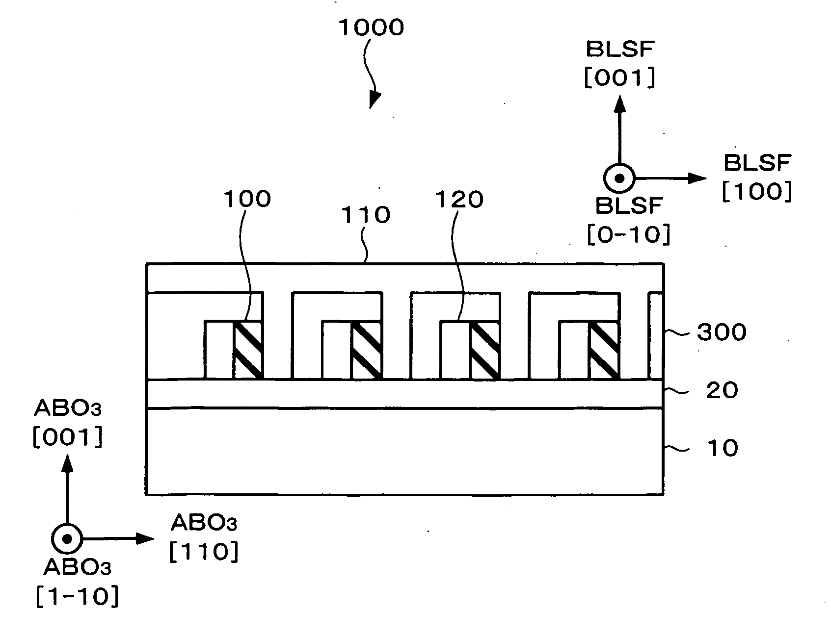
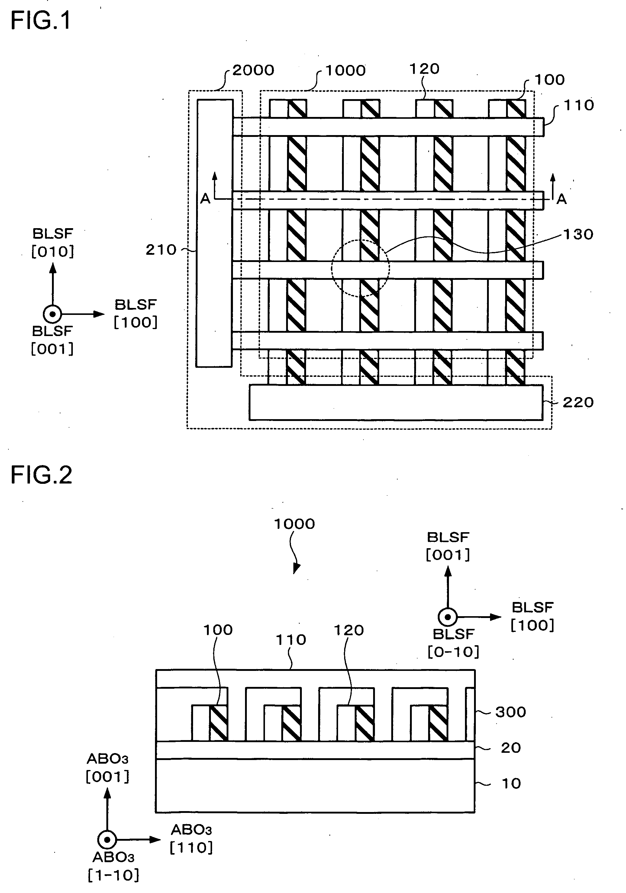
[0034]FIG. 1 is a plan view illustrating a first ferroelectric memory according to an embodiment of the present invention. FIG. 2 is a cross-sectional view of a memory cell array 1000 of the first ferroelectric memory taken along Line A-A of FIG. 1.

[0035] The first ferroelectric memory is a simple matrix type ferroelectric memory comprising a memory cell array 1000 in which memory cells having a ferroelectric capacitor are arranged in a matrix shape and a peripheral circuit section 2000.

[0036] The memory cell array 1000 comprises ferroelectric layers 100, first electrodes 110, and second electrodes 120, which are formed on the substrate 10. The memory cells are formed at intersections 130 between the first electrodes 110 and the second electrodes 120. As shown in the cross-sectional view of FIG. 2, in the memory cell array 1000, an ...


PUM


Abstract

A ferroelectric memory includes a memory cell array in which memory cells having a ferroelectric capacitor are arranged in a matrix shape. The memory cell array includes a ferroelectric layer formed out of a thin film made of a Bi layer-structured ferroelectric single crystal having a (001) orientation and which is patterned such that the ferroelectric layer has two or more side walls perpendicular to a (100) axis of the Bi layer-structured ferroelectrics, first electrodes contacting at least one of the side walls of the ferroelectric layer and which are formed in stripe patterns extending along the one side wall, and second electrodes which contact the other side wall of the ferroelectric layer not contacting the first electrodes and which are formed in stripe patterns to intersect the first electrodes. The memory cells are formed at intersections between the first electrodes and the second electrodes.

Description

RELATED APPLICATIONS [0001] This application claims priority to Japanese Patent Application No. 2004-028997 filed Feb. 5, 2004 which is hereby expressly incorporated by reference herein in its entirety. BACKGROUND [0002] 1. Technical Field [0003] The present invention relates to a ferroelectric memory and a method of manufacturing the ferroelectric memory, and more particularly to a simple matrix type ferroelectric memory employing a Bi layer-structured ferroelectric thin film. [0004] 2. Related Art [0005] A ferroelectric memory is a memory device having the following features: (1) it is nonvolatile, (2) it executes operation at the same switching speed as a volatile memory, and (3) it executes operation with power consumption lower than other memories. [0006] In a Bi layer-structured ferroelectric (BLSF) thin film, crystals tend to be preferentially oriented in a c-axis ((001) axis) direction due to the anisotropic crystal growth. In the Bi layer-structured ferroelectrics, a polari...

Claims


Application Information

Patent Timeline
IPC IPC(8): H01L27/105H01L21/8246H01L27/10H01L29/745
CPCH01L27/101
Inventor KARASAWA, JUNICHIHIGUCHI, TAKAMITSUIWASHITA, SETSUYA
Owner SEIKO EPSON CORP
Learn More