Semiconductor device capable of performing test at actual operating frequency

a technology of a semiconductor device and a test frequency, which is applied in the direction of instruments, coding, code conversion, etc., can solve the problems of inability to detect a malfunction, long time required for testing memory operations, and inability to perform operation tests, so as to avoid performing operation tests, effective detection of delay-associated failures, and convenient conductance

Inactive Publication Date: 2005-09-01
SOCIONEXT INC
View PDF9 Cites 50 Cited by
  • Summary
  • Abstract
  • Description
  • Claims
  • Application Information

AI Technical Summary

Benefits of technology

[0012] According to at least one embodiment of the invention, memory operations are properly tested according to routine instructions issued from the CPU core without using a scan chain. This provides for the test of a memory operation to be readily conducted at an operating frequency of the semiconductor device, without a need for the switching of clocks. This makes it possible to effectively detect a delay-associated failure such as a contact failure that may not come to the surface in an operation test conducted at a low clock rate. Moreover, at least one embodiment of the invention provides for various types of tests to be readily conducted at high speed through simple mani

Problems solved by technology

Because of this, a lengthy time is required for testing memory operations, and it is not possible to detect a malfunction that may occur only when an actual operating frequency is used in the semiconductor device.
Such malfunction may include a malfunction t

Method used


Image

  • Semiconductor device capable of performing test at actual operating frequency
  • Semiconductor device capable of performing test at actual operating frequency
  • Semiconductor device capable of performing test at actual operating frequency

Examples


first embodiment

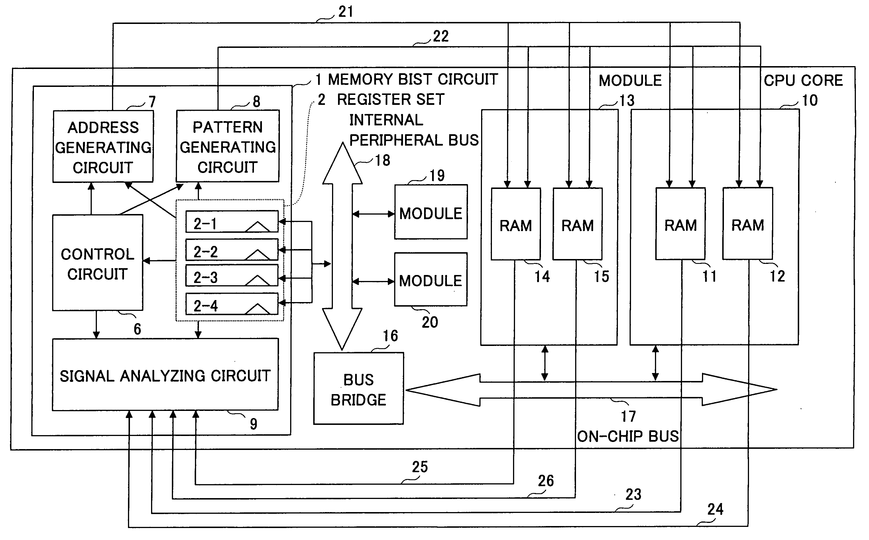
[0033]FIG. 1 is a block diagram showing the construction of a semiconductor device in which a memory BIST circuit is incorporated according to the invention. The semiconductor device of FIG. 1 is a processor that operates at high operating frequency by use of a clock signal output from a PLL, for example, and includes a memory BIST circuit 1, a CPU core 10, a module 13, a bus bridge 16, an on-chip bus 17, an internal peripheral bus 18, a module 19, a module 20, a control signal line 21, a write-data signal line 22, and read-data signal lines 23 through 26. The CPU core 10 includes an instruction cache RAM 11 and a data cache RAM 12. The module 13 includes an in-module RAM 14 and an in-module RAM 15. The memory BIST circuit 1 is provided for the purpose of testing the operations of the instruction cache RAM 11, the data cache RAM 12, the in-module RAM 14, and the in-module RAM 15. For the sake of explanation, a PLL circuit and other circuitries irrelevant to the operation of the memo...

second embodiment

[0052] In the following, the semiconductor device according to the invention will be described.

[0053] When a memory BIST circuit is implemented as a wrapper circuit around a memory as in a conventional configuration, at least one stage of a selector needs to be inserted into a path for memory input / output. If such a selector is inserted into a path leading to a cash RAM of the CPU, it may worsen the timing of a critical path when such a critical path is already critical as to its timing. On the other hand, the provision of signal lines dedicated for use in the memory BIST test results in an undesirable increase in the number of signal lines. In the second embodiment described below, a selector is provided at a location where timing is not critical along a data bus, and the switching of polarities of a test signal allows the memory BIST circuit to access a memory in a pipeline manner.

[0054]FIG. 5 is a block diagram showing an example of the second embodiment of the semiconductor dev...

third embodiment

[0060] In the following, the semiconductor device according to the invention will be described.

[0061] When the operating frequency of a semiconductor device increases from hundreds Mega-hertz to the order of Giga-hertz, the transfer of data between the memory BIST circuit 1 and memories requires an increased time length. As such time length is increased relative to the clock cycle, it becomes difficult to ensure proper operations timing-wise. Especially with the provision of the memory BIST circuit 1 consolidated in a single location, a distance from this location to each memory causes such timing issues to come to the surface. In consideration of this, the third embodiment provides buffer registers (pipeline registers) along a path through which data is supplied from the memory BIST circuit 1 to a memory and along a path through which data is read from the memory to the memory BIST circuit 1, thereby achieving pipeline operations.

[0062]FIG. 6 is a block diagram showing an example ...


PUM


Abstract

A semiconductor device includes a CPU core circuit, a bus connected to the CPU core circuit, and a memory BIST circuit configured to perform a memory test in response to an instruction supplied from the CPU core circuit through the bus.

Description

CROSS-REFERENCE TO RELATED APPLICATIONS [0001] The present application is based upon and claims the benefit of priority from the prior Japanese Patent Application No. 2004-054242 filed on Feb. 27, 2004, with the Japanese Patent Office, the entire contents of which are incorporated herein by reference. BACKGROUND OF THE INVENTION [0002] 1. Field of the Invention [0003] The present invention generally relates to semiconductor devices provided with circuitry for testing a memory, and particularly relates to a semiconductor device provided with a memory BIST circuit for testing a memory and to a voltage control method using a memory BIST circuit. [0004] 2. Description of the Related Art [0005] In semiconductor devices such as processors provided with one or more built-in memories, scan chains are generally used to test the operation of each memory through a limited number of external terminals. The SCAN chain is a chain that allows data to propagate as the data is serially input from an...

Claims


Application Information

Patent Timeline
IPC IPC(8): G11C11/401G01R31/28G11C29/00G11C29/06G11C29/12G11C29/14H01L21/822H01L27/04
CPCG11C29/028G11C29/12015G11C2029/0405G11C29/50012G11C29/14
Inventor SHIKATA, TAKASHI
Owner SOCIONEXT INC
Why Eureka
Try Eureka