Semiconductor device with shallow trench isolation and its manufacture method

Inactive Publication Date: 2005-09-08
FUJITSU SEMICON LTD
View PDF3 Cites 21 Cited by
  • Summary
  • Abstract
  • Description
  • Claims
  • Application Information

AI Technical Summary

Benefits of technology

[0035] A compression stress of the high density plasma oxide film is relaxed by a tensile stress of the silicon nitride film, so that drain current can be increased. A high density plasma oxidation process is executed twice or more and the oxide film on the side wall is removed by a wash-out process inserted between the high density

Problems solved by technology

Namely, a ratio of narrowing the element forming region increases, hindering high integration of semiconductor devices.
Therefore, the distance between the conductive plugs PL and the well 10 under the source/drain regions S/D2 becomes short, resulting in a possibility of leak current by tunneling or the like.
As the opening of a shallow trench becomes narrow, it becomes difficult to completely bury the inside o

Method used


Image

  • Semiconductor device with shallow trench isolation and its manufacture method
  • Semiconductor device with shallow trench isolation and its manufacture method
  • Semiconductor device with shallow trench isolation and its manufacture method

Examples


Embodiment Construction

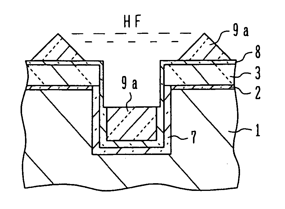
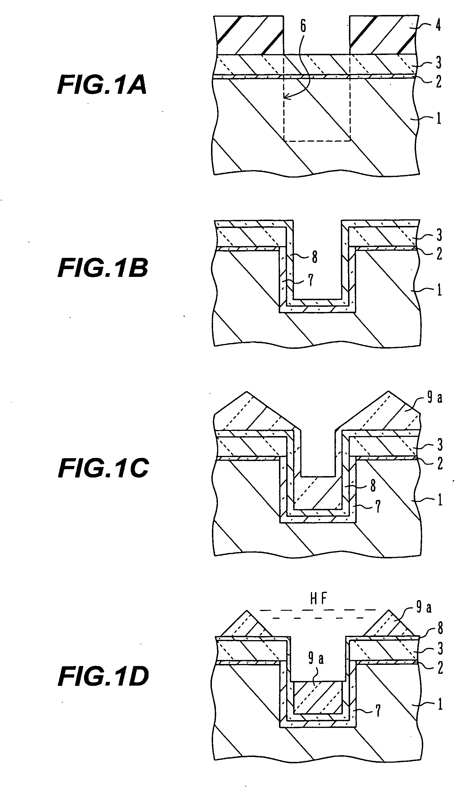
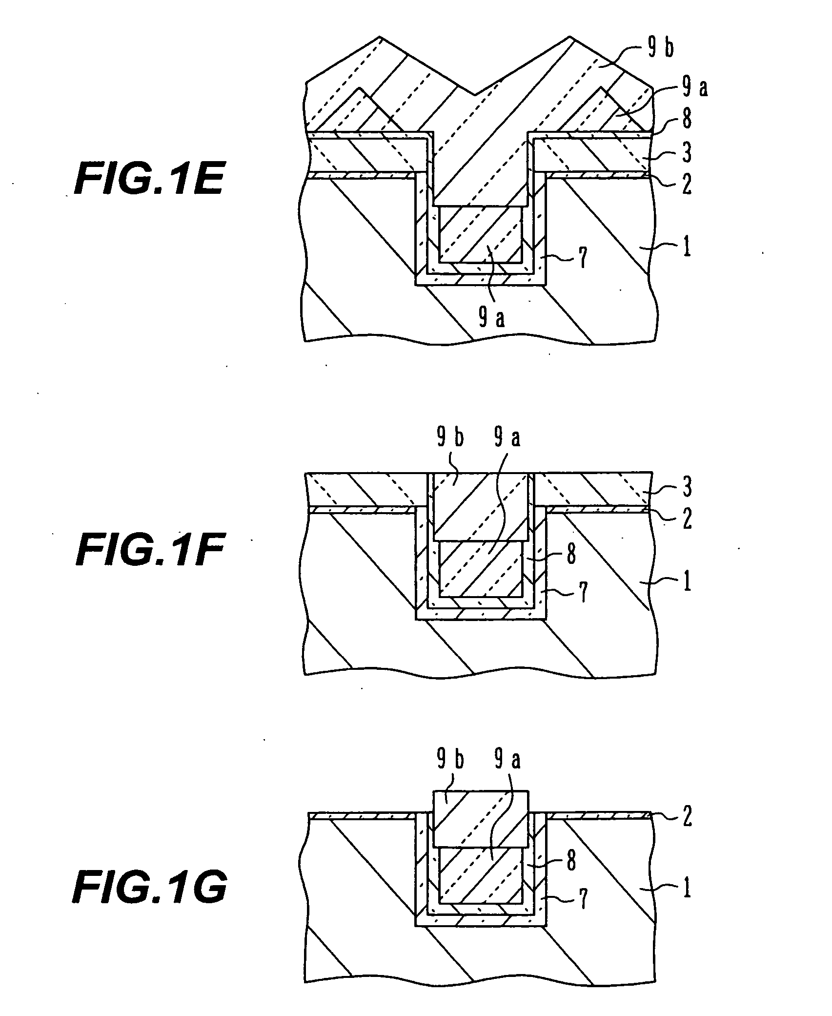
[0041]FIGS. 1A to 1G are cross sectional views of a semiconductor substrate illustrating the main processes of a method of manufacturing a semiconductor device according to an embodiment of the invention.

[0042] As shown in FIG. 1A, the surface of a silicon substrate 1 is wet oxidized at 800° C. to form a buffer oxide film 2 of about 5 nm thick. Next, a silicon nitride layer 3 is formed having a thickness of, for example, 112 nm by chemical vapor deposition (CVD) at a substrate temperature of 775° C. This silicon nitride layer 3 provides a function of a stopper layer during chemical mechanical polishing (CMP). CVD for the silicon nitride layer may use, for example, dichlorosilane and ammonia or the like as the source materials.

[0043] A photoresist mask 4 is formed on the silicon nitride layer 3. This photoresist mask 4 defines a pattern on the active region where an element is formed and has an opening in the region where an element isolation is formed. By using the photoresist pat...


PUM


Abstract

A semiconductor device manufacturing method includes the steps of: (a) forming a stopper layer for chemical mechanical polishing on a surface of a semiconductor substrate; (b) forming an element isolation trench in the stopper layer and the semiconductor substrate; (c) depositing a nitride film covering an inner surface of the trench; (d) depositing a first oxide film through high density plasma CVD, the first oxide film burying at least a lower portion of the trench deposited with the nitride film; (e) washing out the first oxide film on a side wall of the trench by dilute hydrofluoric acid; (f) depositing a second oxide film by high density plasma CVD, the second oxide film burying the trench after the washing-out; and (g) removing the oxide films on the stopper layer by chemical mechanical polishing.

Description

CROSS REFERENCE TO RELATED APPLICATION [0001] This application is based on and claims priority of Japanese Patent Application No. 2004-060210 filed on Mar. 4, 2004, the entire contents of which are incorporated herein by reference. BACKGROUND OF THE INVENTION [0002] A) Field of the Invention [0003] The present invention relates to a semiconductor device and its manufacture method, and more particularly to a semiconductor device having shallow trench isolation (STI) and its manufacture method. [0004] B) Description of the Related Art [0005] Local oxidation of silicon (LOCOS) is known as one of element isolation methods for semiconductor devices. [0006] According to the technique of local oxidation of silicon, after a silicon oxide film is formed on a silicon substrate as a buffer layer, a silicon nitride film is formed as an oxidation preventing mask layer, and after the silicon nitride film is patterned, the surface of the silicon substrate is thermally oxidized via the silicon oxid...

Claims


Application Information

Patent Timeline
IPC IPC(8): H01L21/31H01L21/76H01L21/74H01L21/762H01L27/08H01L29/78H01L31/113
CPCH01L21/31053H01L21/31111H01L29/7833H01L21/823878H01L21/76232
Inventor INOUE, KENGOOTA, HIROYUKI
Owner FUJITSU SEMICON LTD
Why Eureka
Try Eureka