Laser crystallization apparatus and laser crystallization method

a laser crystallization and crystallization apparatus technology, applied in semiconductor lasers, semiconductor/solid-state device testing/measurement, instruments, etc., can solve the problems of inconvenient use, inconvenient observation of the changing silicon film from melting to crystallization through images with high temporal resolution and/or high spatial resolution

Inactive Publication Date: 2005-09-15
ADVANCED LCD TECH DEVMENT CENT
View PDF7 Cites 27 Cited by
  • Summary
  • Abstract
  • Description
  • Claims
  • Application Information

AI Technical Summary

Benefits of technology

[0023] Problems and concerns described above can be solved by a laser crystallization apparatus and a laser crystallization method set forth below.

Problems solved by technology

However, as compared with the stability of the excimer laser light, a process margin to form a crystallized silicon thin film having a predetermined quality is extremely narrow.
Problems in industrializing a mass production line for crystallization utilizing an ELA apparatus used here include improvement in yield of a crystallization process, and stabilization in quality control by monitoring the crystallization process by an operator due to instabilities of irradiating laser light, such as missing of a pulse and / or fluctuation in the intensity, for example.
The method in the Jpn. Pat. Appln. KOKAI Publication No. 2001-257176 described above is not suitable for the purpose of observing the crystallization of the silicon thin film through images.
The method in the Jpn. Pat. Appln. KOKAI Publication No. 2002-176009 is available for observing through images, however it is not suitable for observing the changing silicon film from melting to crystallization through images with the high temporal resolution and / or high spatial resolution.
The method of M. Hatano et al. has high resolution in time, but is not applicable to an image observation system that satisfies both the high spatial resolution of several μm or less and the high temporal resolution of several nsec at the same time.
When the wavelengths of these laser lights are taken into account, lens materials that can preferably be used are limited to UV-grade synthetic quarts or calcium fluoride (CaF2), which reduces the freedom in lens designing.
When the excimer laser light and the microscopic observation visible light are used in this single optical system, the aberration correction has to be made simultaneously in two wavelength areas including the ultraviolet light and the visible light, which is a significantly difficult problem.
Another problem is that the crystallization optical system adapted to the excimer laser light with the above-described performance reduces the resolution of the visible light when it transmits the visible light.
As a result, it cannot be obtained a resolution of 1 μm necessary to observe or measure the images of the crystallized area of several μm.
The lens sufficiently satisfies the desire with the spatial resolution (1 μm), but is not capable of an operation with the above-described high light intensity, large irradiation area and high duty.
If the visible light is applied as such illumination light for observation through a large number of optical lenses, this causes not only a problem of loss in amount of light but also a problem of an adverse effect on the imaging performance of the original ultraviolet light.

Method used


Image

  • Laser crystallization apparatus and laser crystallization method
  • Laser crystallization apparatus and laser crystallization method
  • Laser crystallization apparatus and laser crystallization method

Examples


Embodiment Construction

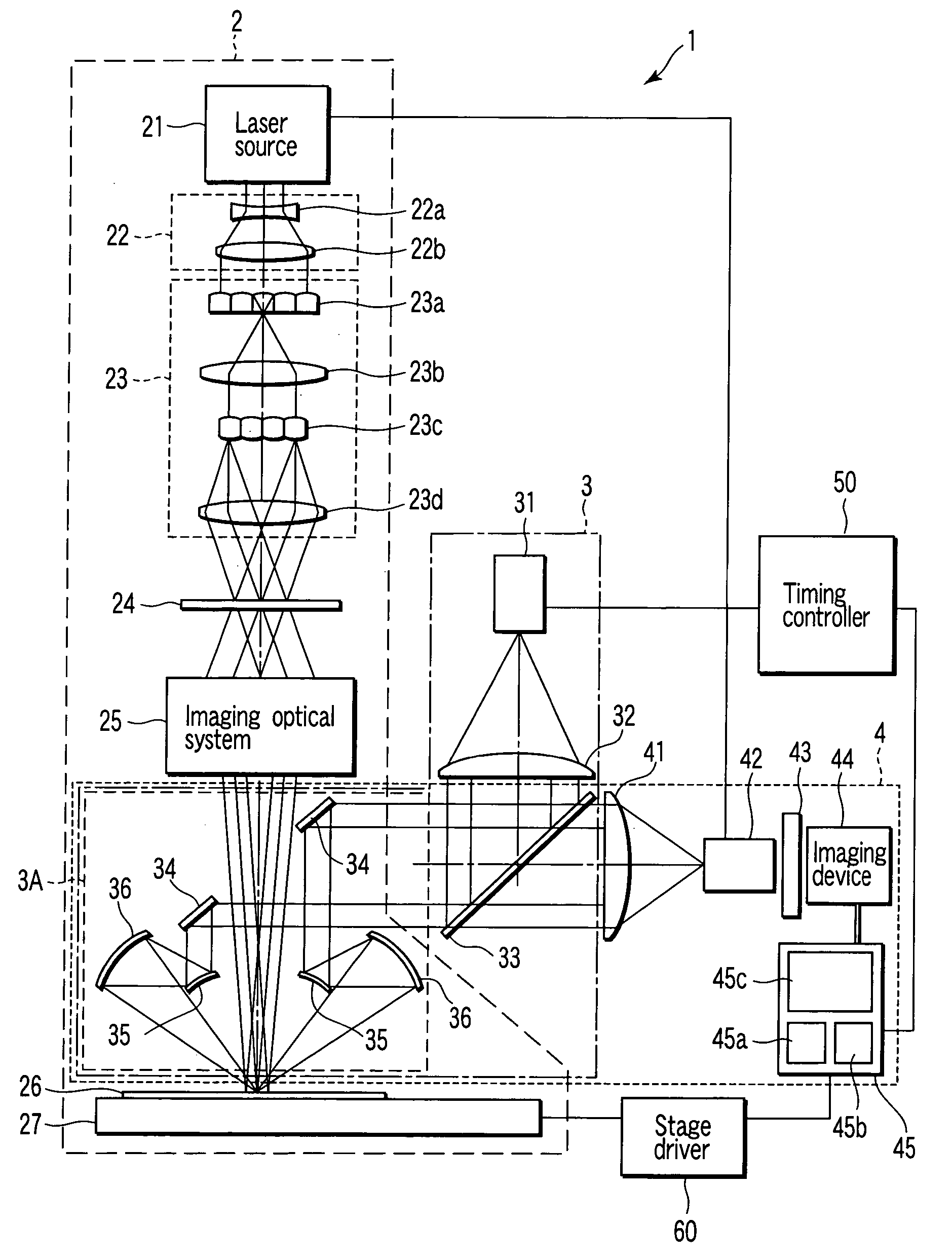
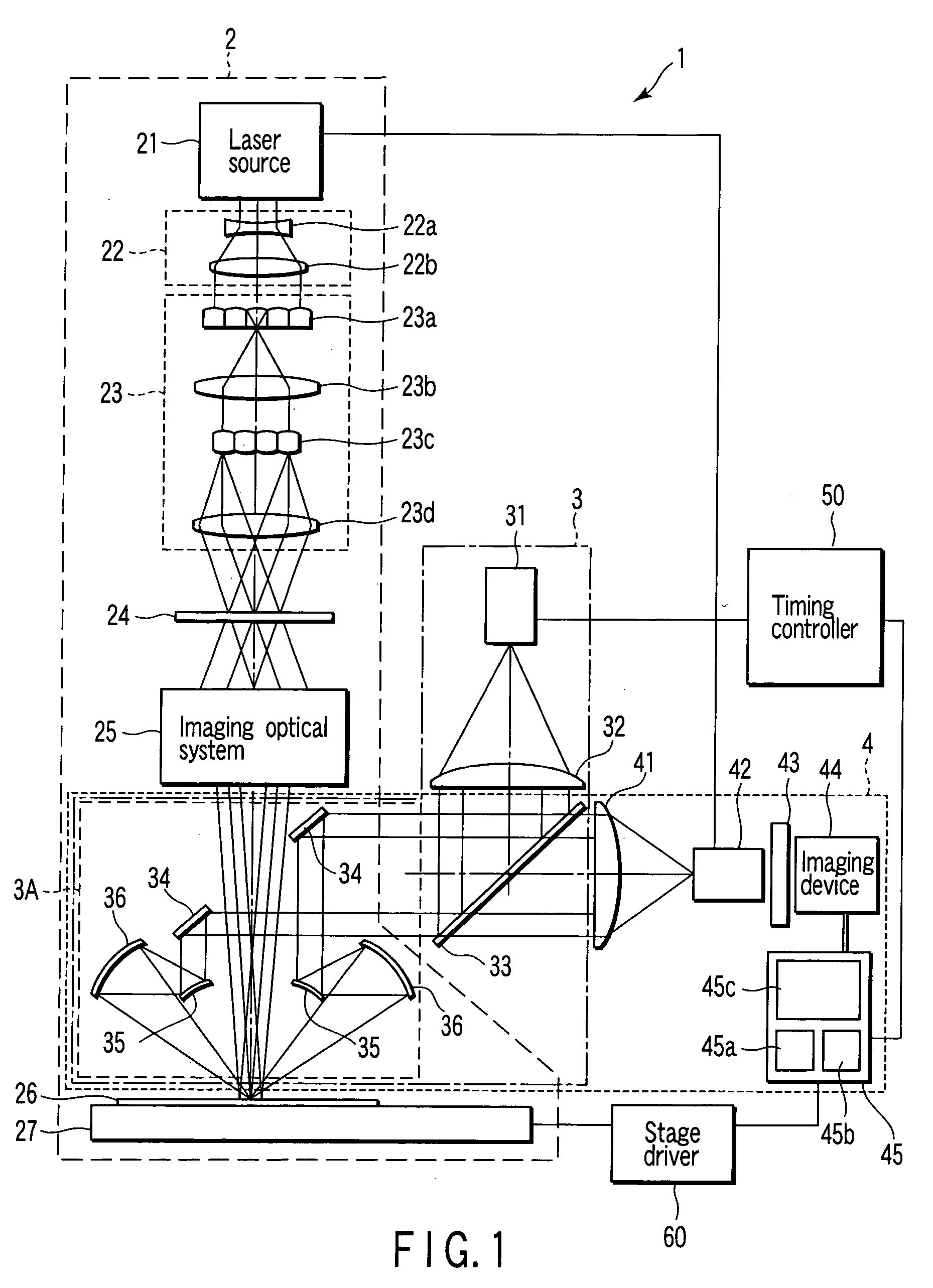
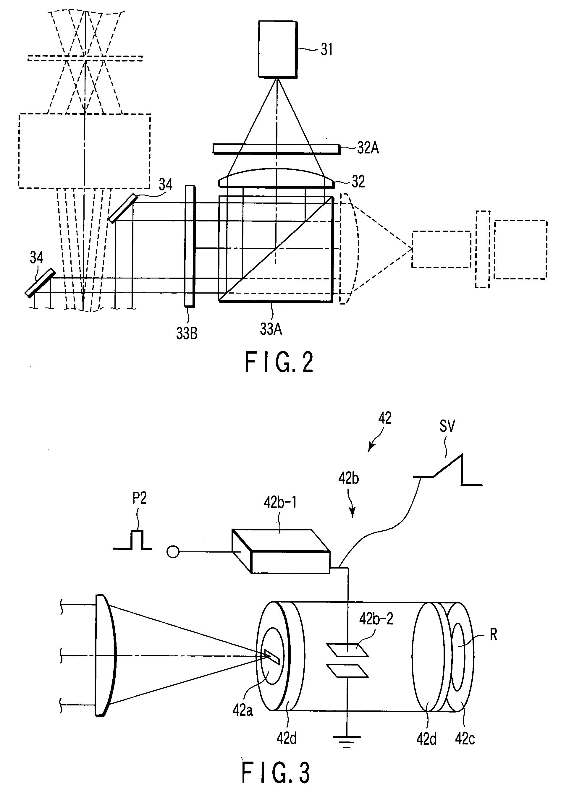
[0035] The embodiments of the present invention will be described with reference to the accompanying drawings. The accompanying drawings, which are incorporated in and constitute a part of the specification, illustrate embodiments of the invention, and together with the general description given above and the detailed description of the embodiments given below, serve to explain principles of the invention. Throughout the drawings, corresponding portions are denoted by corresponding reference numerals. The embodiments are only examples, and various changes and modifications can be made without departing from the scope and spirit.

[0036] In an ELA apparatus, to observe or measure images of a crystallization process area of several μm in real time where a semiconductor thin film is melted and crystallized in several hundreds nsec, it is necessary to manage both demands from an excimer laser crystallization optical system for crystallization and from a microscopic observation system for...


PUM

PropertyMeasurementUnit
wavelengthsaaaaaaaaaa

Abstract

A laser crystallization apparatus, which enables an observation of a high spatial resolution with several μm and a high temporal resolution with several nanoseconds, comprising a crystallization optical system to irradiate a laser light to a thin film provided on a substrate and to melt and crystallize the thin film, the laser crystallization apparatus comprises an illumination light source disposed out of an optical path of the laser light and emitting an illumination light for observation to illuminate the thin film, an illumination optical system comprising an annular optical element which has the optical path of the laser light in the center and which leads the illumination light from the illumination light source to the thin film along the optical path, and an observation optical system which displays a magnified image of the substrate including the thin film.

Description

CROSS-REFERENCE TO RELATED APPLICATIONS [0001] This application is based upon and claims the benefit of priority from prior Japanese Patent Applications No. 2004-069470, filed Mar. 11, 2004; and No. 2004-351734, filed Dec. 3, 2004, the entire contents of both of which are incorporated herein by reference. BACKGROUND OF THE INVENTION [0002] 1. Field of the Invention [0003] The present invention relates to a crystallization apparatus which irradiates laser light-to a thin film such as a semiconductor film and to a crystallization method, and more specifically to a laser crystallization apparatus and a laser crystallization method in which melting and crystallization process of the semiconductor film can be observed in a magnified image in real time. [0004] 2. Description of the Related Art [0005] A laser crystallization technology has been developed, in which, for example, a high-energy short-pulse laser light is used to melt and crystallize a semiconductor thin film to make a non sin...

Claims


Application Information

Patent Timeline
Patent Type & Authority Applications(United States)
IPC IPC(8): H01L21/20H01L21/268
CPCH01L21/02678H01L21/02686H01L22/12H01L22/26H01L21/268H01L2924/0002B23K26/0042B23K26/032H01L2924/00B23K26/0006B23K2103/56H01S3/10H01S5/00
Inventor TAKAMI, YOSHIO
Owner ADVANCED LCD TECH DEVMENT CENT
Why Eureka
Try Eureka