Laser micromachining using programmable pulse shapes

a technology of programmable pulses and micro-machining, which is applied in the direction of manufacturing tools, instruments, optics, etc., can solve the problems of ic reliability problems, limit the option of having adjustable pulse width and pulse shape, and excess removal, so as to reduce risk, improve throughput, and reduce damage to pcb copper pads

Inactive Publication Date: 2009-10-01
ELECTRO SCI IND INC
View PDF17 Cites 54 Cited by
  • Summary
  • Abstract
  • Description
  • Claims
  • Application Information

AI Technical Summary

Benefits of technology

[0006]Tailored pulses are useful in laser processing applications, such as laser printed circuit board (PCB) via drilling to achieve better throughput and less damage to the PCB copper pads, and laser link processing to reduce risk of generating over-craters in the overlying passivation layer. Preferred embodiments are implemented with one or more electro-optical modulators receiving drive signals that selectively change the amount of incident pulsed laser emission to form a tailored pulse output. Triggering the drive

Problems solved by technology

Conventional lasers generally limit the option of having adjustable pulse width and pulse shape.
A traditional longer leading edge rise time of a 5 ns-10 ns wide laser pulse could result in excess removal of (“over-crater in”) the overlying passivation layer material during link processing, especially when the overlying passivation layer is too thick or varies over a wide range across a wafer or among a group of wafers.
Some laser link processes using traditional laser pulses with pulse widths of a few nanoseconds to a few tens of nanoseconds tend to over-crater in thicker overlying

Method used


Image

  • Laser micromachining using programmable pulse shapes
  • Laser micromachining using programmable pulse shapes
  • Laser micromachining using programmable pulse shapes

Examples


Embodiment Construction

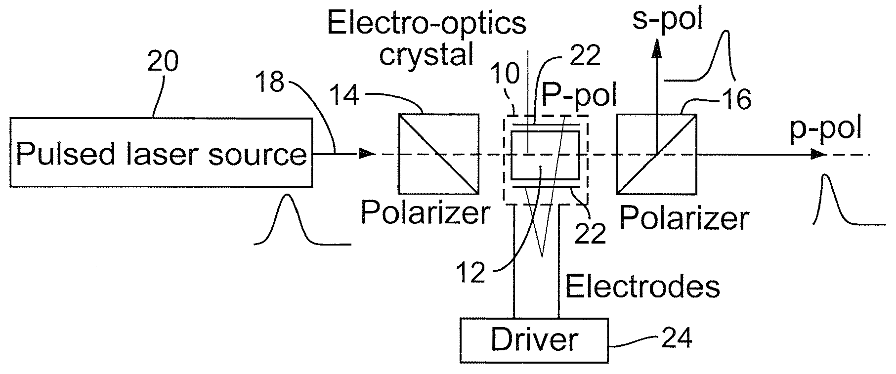
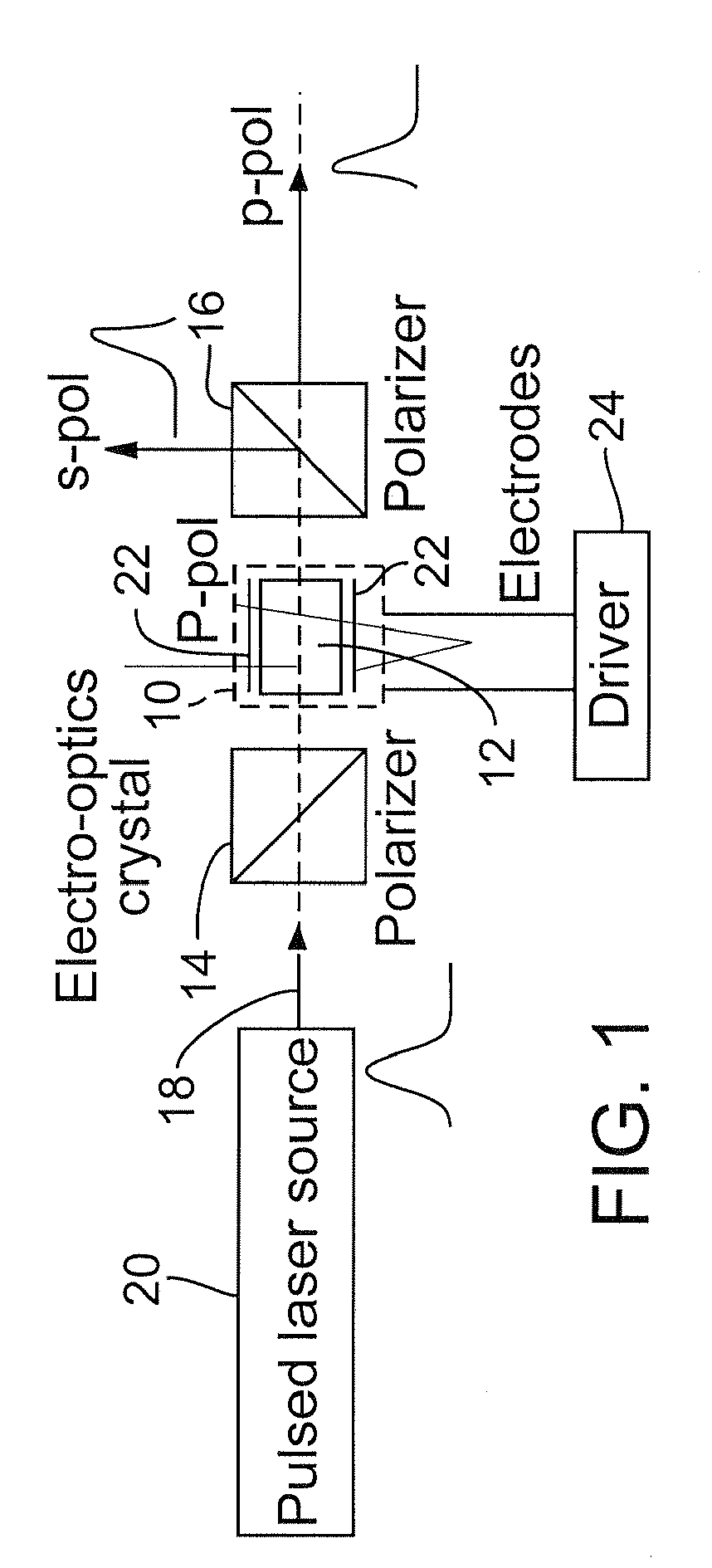
[0026]FIG. 1 shows an electro-optical modulator 10 that is implemented in a number of laser pulse slicing system embodiments described below to produce tailored laser pulse output. Electro-optical modulator 10 includes an electro-optical crystal 12 cell that is positioned between light polarizing devices (polarizers) 14 and 16 and receives a beam of laser pulses 18 emitted by a pulsed laser source 20. Electro-optical crystal cell 12 has electrodes 22 to which drive output signals of driver circuitry 24 are applied to contribute to shaping of incident laser pulses 18. Laser source 20 can be any pulsed laser emitting a laser pulse of a pulse width within a range of a few nanoseconds to 100 ns. Electro-optical crystal cell 12 can be made of KDP, KD*P, ADP, AD*P, RTP, RTA, BBO, LiNbO3, or other electro-optical materials. One example of a suitable electro-optical crystal cell 12 is a LightGate 4 BBO Pockels cell manufactured by Cleveland Crystals, Inc., Highland Heights, Ohio. The LightG...


PUM

PropertyMeasurementUnit
Electrical conductivityaaaaaaaaaa
Poweraaaaaaaaaa
Electrical resistanceaaaaaaaaaa

Abstract

Laser pulse shaping techniques produce tailored laser pulse spectral output. The laser pulses can be programmed to have desired pulse widths and pulse shapes (such as sub-nanosecond to 10 ns-20 ns pulse widths with 1 ns to several nanoseconds leading edge rise times). Preferred embodiments are implemented with one or more electro-optical modulators receiving drive signals that selectively change the amount of incident pulsed laser emission to form a tailored pulse output. Triggering the drive signal from the pulsed laser emission suppresses jitter associated with other stages of the link processing system and substantially removes jitter associated with pulsed laser emission build-up time.

Description

BACKGROUND INFORMATION[0001]Many laser micromachining processes require laser pulses of various shapes. For example, laser processing of multiple layers of different materials demands fairly large adjustable ranges of laser power, pulse repetition rate, pulse width, spot size, and pulse shape to achieve either or both of desired quality and throughput. With a conventional Q-switched laser, all of the parameters can be adjusted over only limited ranges, especially the pulse width and pulse shape. Conventional lasers generally limit the option of having adjustable pulse width and pulse shape. As another example, the processing of electrically conductive links on memory chips or other integrated circuit (IC) chips demands pulses with a fairly short leading edge rise time (e.g., 1 ns-2 ns rise time) to achieve desired quality and yield. With existing solid-state lasers, the leading edge rise time changes with pulse width. A traditional longer leading edge rise time of a 5 ns-10 ns wide ...

Claims


Application Information

Patent Timeline
IPC IPC(8): H01S3/10H01S3/00
CPCB23K26/063H01S3/0057G02F1/0327B23K26/0622
Inventor PENG, XIAOYUANBAIRD, BRIAN W.JORDENS, WILLIAM J.HEMENWAY, DAVID MARTIN
Owner ELECTRO SCI IND INC
Why Eureka
Try Eureka