Laser micromachining with tailored bursts of short laser pulses

a laser pulse and laser micromachining technology, applied in lasers, manufacturing tools, welding/soldering/cutting articles, etc., can solve problems such as “over crater”, reduce the reliability of ic chips, and non-optimal thickness

Active Publication Date: 2010-09-30
ELECTRO SCI IND INC
View PDF44 Cites 55 Cited by
  • Summary
  • Abstract
  • Description
  • Claims
  • Application Information

AI Technical Summary

Benefits of technology

[0012]A series of laser pulse bundles or bursts are used for micromachining target structures. The target structures may be on or in semiconductor devices, for example, that have multiple layers. Each burst includes short laser pulses with temporal pulse widths that are less than approximately 1 nanosecond. In some embodiments, each laser pulse has a temporal pulse width in a range between approximately 1 nanosecond and approximately 100 femtoseconds.

Problems solved by technology

Use of a traditional Gaussian-shaped laser pulse having a 5-20 nanosecond pulse width and a sloped, gradually rising front edge in link processing tends to cause an “over crater” in the passivation layer, especially if its thickness is too large or is uneven.
Over cratering reduces the reliability of IC chips.
Difficulty in maintaining wafer-level process control of the passivation layer during IC fabrication may result in non-optimal thickness and poor cross-wafer or wafer-to-wafer thickness uniformity.
However, generating a pulsed laser from a CW light beam is fairly inefficient, and thus requires more amplification.
Because such a low peak-power signal may be influenced by noise, which causes pulse-to-pulse instability, the two modulators are preferably synchronized to maintain pulse stability and energy stability, thereby adding further complexity and cost.
However, laser pulses with pulse widths in the nanosecond range have disadvantages.
Such a conventional link processing laser pulse creates a large heat affected zone (HAZ) that could deteriorate the quality of the device that includes the severed link.
Increased laser pulse energy increases the damage risk to the IC chip, including irregular or over sized opening in the overlying passivation layer, cracking in the underlying passivation layer, damage to the neighboring link structure and damage to the silicon (Si) substrate.
However, using laser pulse energy within a risk-free range on thick links often results in incomplete link severing.
However, the high peak power of a single ultrafast pulse may easily damage the underlying Si substrate, which is unacceptable in many applications.
A problem with using a train of ultrafast pulses is that many commercially available ultrafast lasers that use a pulse picker have pulse repetition rates in the 1 kHz to 200 kHz range.
Such a repetition rate may be difficult to be directly applied to links because stage movement, typically approximately 400 mm / s, is too slow to move the “next” laser pulse to the “next” link within the laser pulse interval time of a few tens of nanoseconds.

Method used


Image

  • Laser micromachining with tailored bursts of short laser pulses
  • Laser micromachining with tailored bursts of short laser pulses
  • Laser micromachining with tailored bursts of short laser pulses

Examples


Embodiment Construction

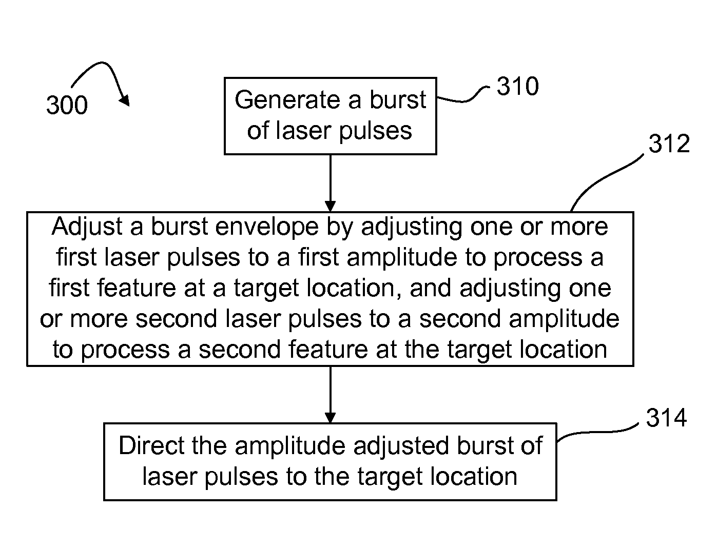
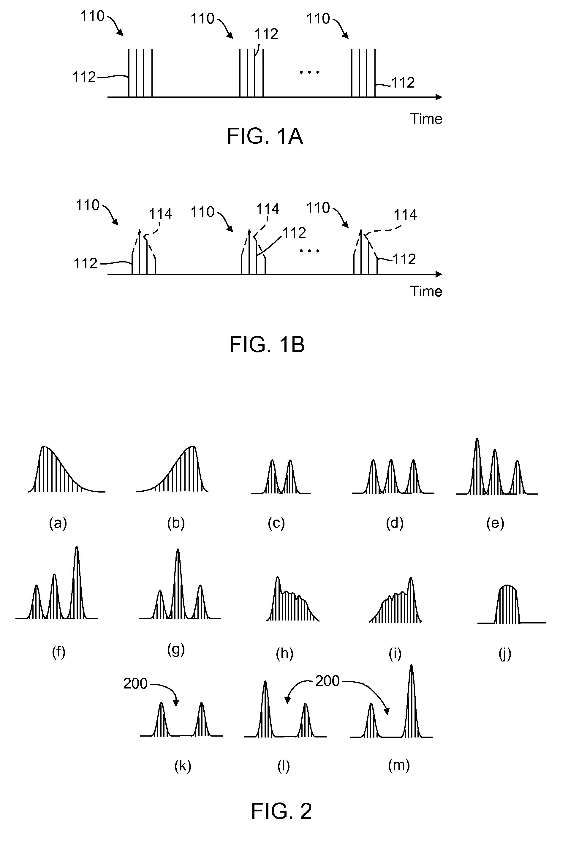
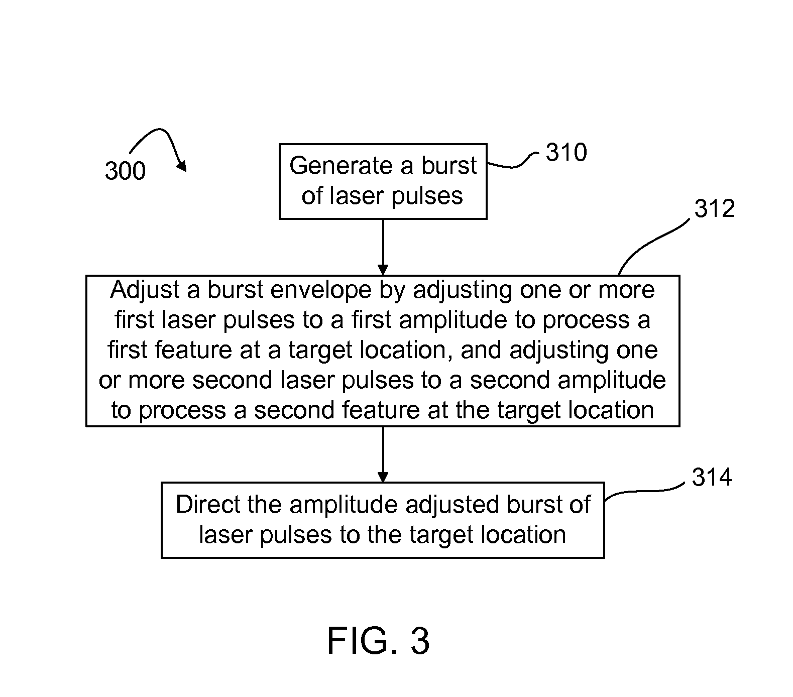
[0031]In certain embodiments, a series of laser pulse bundles or bursts are used for micromachining target structures. The target structures may be on or in semiconductor devices, for example, that have multiple layers with different laser processing characteristics. Or, the target structures may include a single material that has multiple laser processing characteristics. For example, a top surface of the material, a bulk or inner portion of the material, and a bottom surface of the material may have different laser processing characteristics. Further, the laser processing characteristics may vary at different depths within the material.

[0032]Each burst includes short laser pulses with temporal pulse widths that are less than approximately 1 nanosecond. In some embodiments, each laser pulse has a temporal pulse width in a range between approximately 1 nanosecond and approximately 100 femtoseconds. Temporal pulse widths that are less than approximately 10 picoseconds may be referred...


PUM

PropertyMeasurementUnit
wavelengthsaaaaaaaaaa

Abstract

A series of laser pulse bundles or bursts are used for micromachining target structures. Each burst includes short laser pulses with temporal pulse widths that are less than approximately 1 nanosecond. A laser micromachining method includes generating a burst of laser pulses and adjusting an envelope of the burst of laser pulses for processing target locations. The method includes adjusting the burst envelope by selectively adjusting one or more first laser pulses within the burst to a first amplitude based on processing characteristics of a first feature at a target location, and selectively adjusting one or more second laser pulses within the burst to a second amplitude based on processing characteristics of a second feature at the target location. The method further includes directing the amplitude adjusted burst of laser pulses to the target location.

Description

TECHNICAL FIELD [0001]The present disclosure relates to laser micromachining. In particular, the present disclosure relates to laser systems and methods that use a tailored burst of short or ultrashort laser pulses.BACKGROUND INFORMATION [0002]Laser micromachining processes include, for example, semiconductor memory link processing, material trimming, wafer / panel scribing, wafer / panel dicing, and via drilling. Generally, laser micromachining may use laser pulses having wavelengths of, for example, 1.3 μm, 1.064 μm, 1.053 μm, or 1.047 μm, and their harmonics, and pulse widths in a nanosecond range (e.g., between a few nanoseconds and approximately 200 nanoseconds), depending on the particular materials and target structure to be processed, the laser sources used, and the pulse repetition rates used. Laser micromachining processes such as wafer dicing, for example, may use mode-locked laser pulses with pulse widths that are less than approximately 1 nanosecond and pulse repetition rat...

Claims


Application Information

Patent Timeline
Patent Type & Authority Applications(United States)
IPC IPC(8): H01S3/098H01S3/10
CPCB23K26/063B23K26/0635B23K26/403B23K26/4065B23K2203/12B23K26/408B23K26/409B23K2203/10B23K26/4075
Inventor SUN, YUNLONG
Owner ELECTRO SCI IND INC
Why Eureka
Try Eureka