Nonvolatile semiconductor memory device and manufacturing method thereof

a nonvolatile, memory device technology, applied in the direction of semiconductor devices, electrical devices, transistors, etc., can solve the problems of increasing the amount of unerased electrons, the inability to secure the prescribed threshold voltage, and the inability to shorten the erasing time by leaps and bounds, so as to reduce the number of unerased electrons, improve rewriting durability, and reduce the influence of unerased and remaining electrons

Active Publication Date: 2005-09-15
RENESAS ELECTRONICS CORP
View PDF3 Cites 41 Cited by
  • Summary
  • Abstract
  • Description
  • Claims
  • Application Information

AI Technical Summary

Benefits of technology

[0037] As the present invention is outlined on the basis of the examples of the three kinds of typical configurations in the above explanations, the essential point of the present invention is: to remove the entire Si nitride film on the select gate electrode sidewall as explained in the example of the first configuration (FIG. 18); to remove a part of the Si nitride film on the select gate electrode sidewall as explained in the example of the second configuration (FIG. 19); or to control the thickness of the Si nitride film on the select gate electrode sidewall so as to be thinner than that of the other region (between the memory gate MG and the semiconductor substrate) and to lessen the influence of the unerased and remaining electrons as explained in the example of the third configuration (FIG. 20).
[0038] By the present invention, it becomes possible to remarkably reduce the number of unerased electrons caused by hot-hole erasing and to improve rewriting durability.
[0039] Further, by the present invention, since the erasing time by hot holes is largely shortened, it is possible to reduce the erasing current required for erasing. By so doing, the area of a power supply circuit is reduced and the production cost is also reduced.
[0040] Furthermore, by the present invention, since the erasing time is largely shortened, it is possible to restrain the deterioration of the lower layer potential barrier film (bottom Si oxide film) accompanying erasing. By so doing, the electric charge retention capability improves.
[0041] As a result of combining all above effects, the present invention makes it possible to realize a MONOS nonvolatile memory of a split gate structure excellent in rewriting durability and an electric charge retention capability at a low cost.

Problems solved by technology

In addition, since the MONOS method does not see the radical shortening of charge retention time caused by defects of an Si oxide film, hot-hole erasure which is likely to cause damage to an Si oxide film can be adopted, thus erasing time can be shortened by leaps and bounds, and resultantly the MONOS method gathers attention in recent years.
The amount of unerased electrons increases as the frequency of rewriting increases, and therefore the drawback here is that a prescribed threshold voltage cannot be secured even though erasing of electrons is carried out for the last time.

Method used


Image

  • Nonvolatile semiconductor memory device and manufacturing method thereof
  • Nonvolatile semiconductor memory device and manufacturing method thereof
  • Nonvolatile semiconductor memory device and manufacturing method thereof

Examples


embodiments

[0070] Next, the example of the first configuration explained earlier in FIG. 18 is explained concretely on the basis of the first and second embodiments, the example of the second configuration explained earlier in FIG. 19 on the basis of the third embodiment, and the example of the third configuration explained earlier in FIG. 20 on the basis of the fourth embodiment.

first embodiment

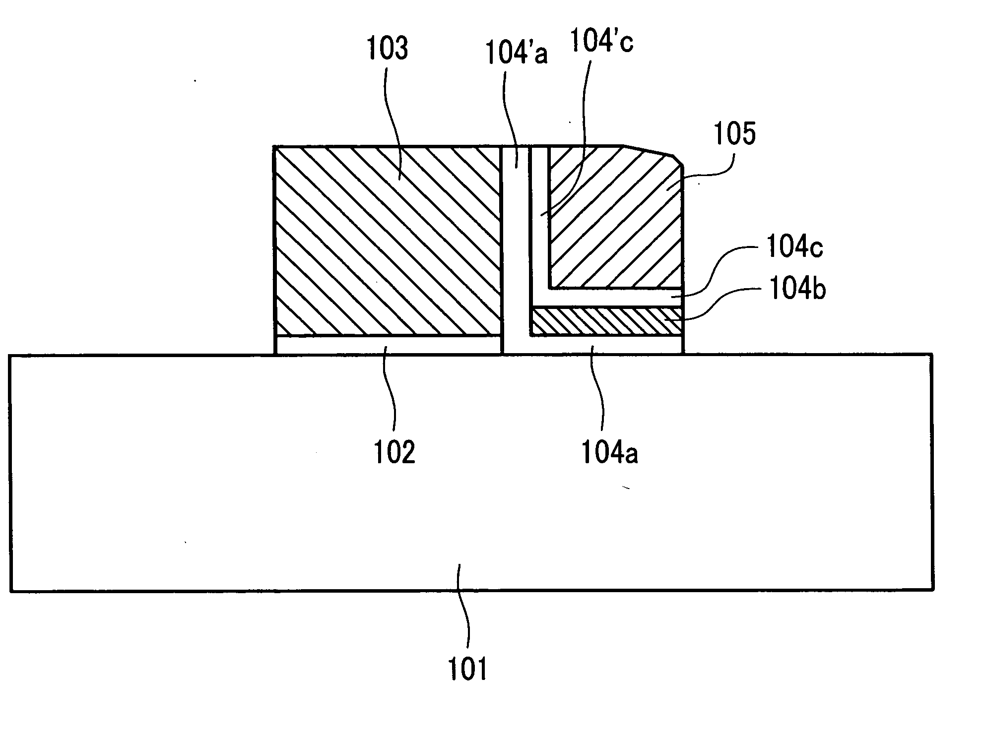
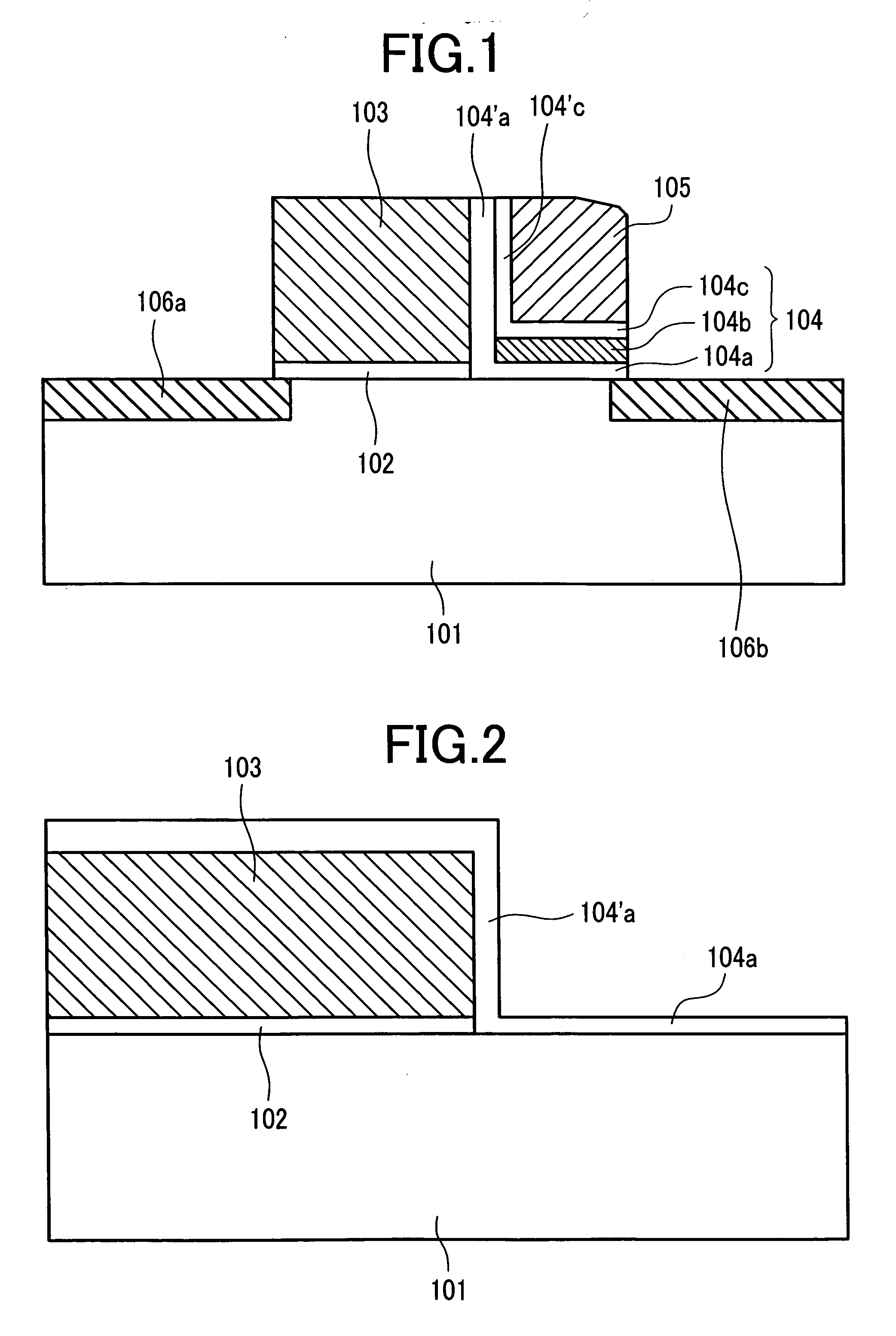
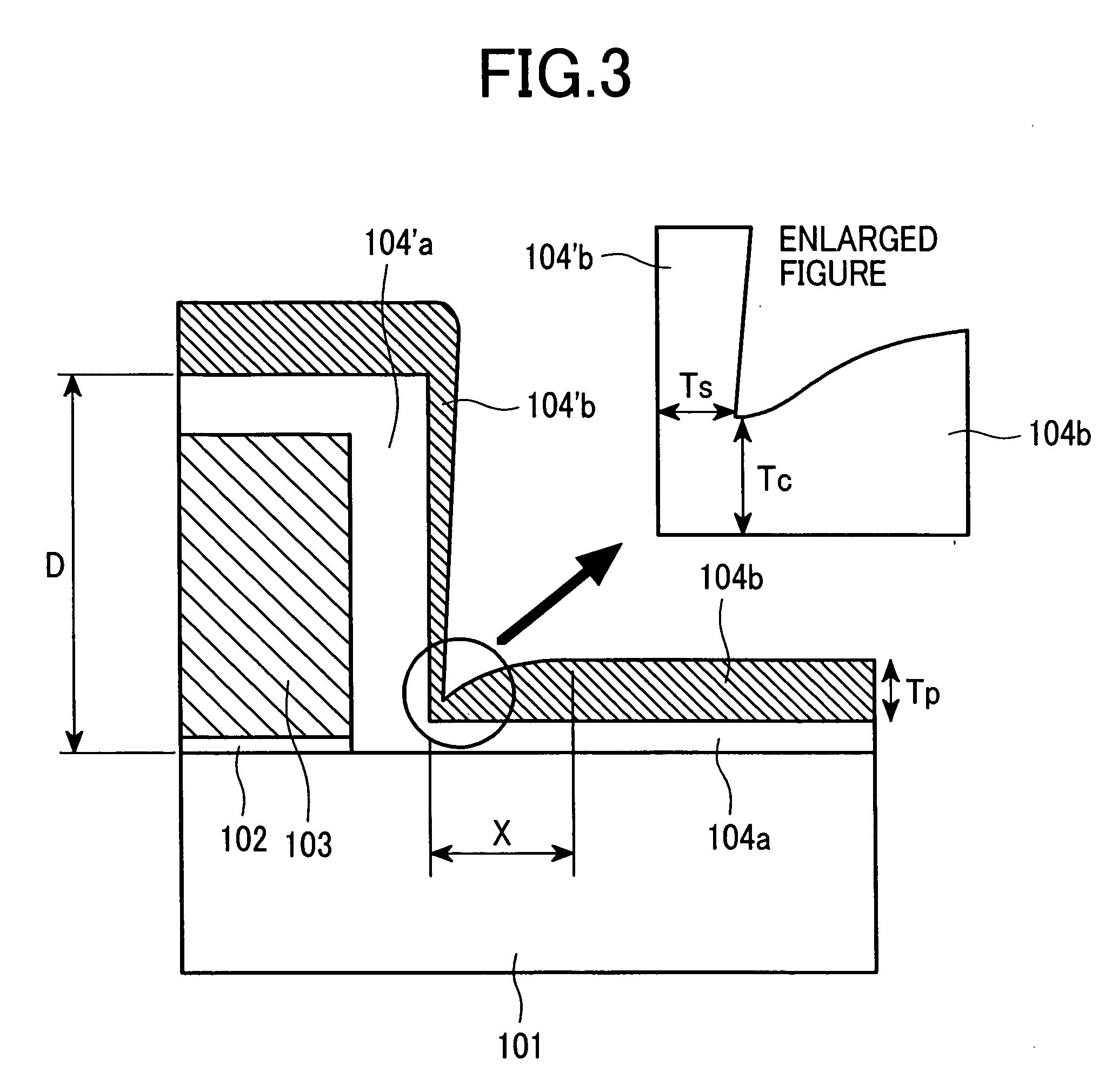
[0071]FIG. 1 is a sectional view of the first embodiment according to the present invention and corresponds to a sectional view taken on line X-Y of FIG. 7. The bit line 17 is expressed in FIG. 7 but not in FIG. 1.

[0072] The MONOS memory cell of a split gate structure produced in the present embodiment is composed of: a p-type well region (Si substrate) 101 formed on an Si substrate (semiconductor substrate); and two MOS transistors Q1 and Q2 having an n-type diffusion layer (n-type semiconductor region) acting as a source region 106a and another n-type diffusion layer acting as a drain region 106b, respectively.

[0073] The select MOS transistor Q2 is composed of an Si oxide film acting as a gate insulator film 102 and an n-type polycrystalline silicon film (hereunder referred to as “Si film”) acting as a select gate electrode (electric conductor) 103.

[0074] The memory MOS transistor Q1 is composed of: an Si oxide film acting as a lower layer potential barrier film 104a isolating ...

second embodiment

[0095] Next, the second embodiment according to the present invention is explained on the basis of FIGS. 21 to 26. In the embodiment, in the same way as the first embodiment, three other methods wherein an Si nitride film acting as a charge trapping film was not formed at the sidewall bottom portion of the select gate electrode were investigated. The obtained results are hereunder explained sequentially.

[0096] (1) The First Method

[0097] The method is explained on the basis of FIGS. 21 and 22. Firstly, as shown by the sectional view of FIG. 21, the gate insulator film 802 of the select MOS transistor Q2 was formed on the Si substrate 801 in the same way as the first embodiment, and thereafter the non-doped polycrystalline Si film 803 200 nm in thickness was deposited.

[0098] Successively, phosphor was injected by 8e15 atms / cm2 into the region 803″ about 100 nm distant from the surface of the polycrystalline Si film 803 acting as the select gate electrode 803 by the ion implantation...


PUM


Abstract

A MONOS nonvolatile memory of a split gate structure, wherein writing and erasing are performed by hot electrons and hot holes respectively, is prone to cause electrons not to be erased and to remain in an Si nitride film on a select gate electrode sidewall and that results in the deterioration of rewriting durability. When long time erasing is applied as a measure to solve the problem, drawbacks appear, such as the increase of a circuit area caused by the increase of the erasing current and the deterioration of retention characteristics. In the present invention, an Si nitride film is formed by the reactive plasma sputter deposition method that enables oriented deposition and the Si nitride film on a select gate electrode sidewall is removed at the time when a top Si oxide film is formed.

Description

CLAIM OF PRIORITY [0001] The present application claims priority from Japanese application JP 2004-066767 filed on Mar. 10, 2004, the content of which is hereby incorporated by reference into this application. FIELD OF THE INVENTION [0002] The present invention relates to the structure of a nonvolatile semiconductor memory device and its manufacturing method, in particular to a highly reliable nonvolatile semiconductor memory device capable of low voltage operation and high-speed programming and its manufacturing method. BACKGROUND OF THE INVENTION [0003] It becomes possible to realize a highly functional semiconductor device by consolidating a nonvolatile semiconductor memory cell with a logic semiconductor device on the same silicon (Si) substrate. Such highly functional semiconductor devices are widely used as built-in microcomputers for industrial machines, home appliances, vehicle-installed devices, and others. [0004] A consolidated nonvolatile memory is generally used by stori...

Claims


Application Information

Patent Timeline
Patent Type & Authority Applications(United States)
IPC IPC(8): H01L27/115H01L21/8247H01L29/04H01L29/788H01L29/792
CPCH01L21/28282H01L29/792H01L27/11568H01L29/40117H10B43/30
Inventor MINE, TOSHIYUKIYOKOYAMA, NATSUKIYASUI, KAN
Owner RENESAS ELECTRONICS CORP
Why Eureka
Try Eureka