Method to manufacture polymer memory with copper ion switching species

a technology of copper ions and polymer memory, applied in the direction of digital storage, instruments, electrical equipment, etc., can solve the problems of shortening the data holding time of elements, ram devices are typically volatile, and the storage data is lost, so as to achieve flexibility in memory system design and easy and inexpensive manufacturing

Inactive Publication Date: 2005-09-15
MICRON TECH INC
View PDF14 Cites 7 Cited by
  • Summary
  • Abstract
  • Description
  • Claims
  • Application Information

AI Technical Summary

Benefits of technology

[0008] Embodiments of the present invention provide molecular memory cells and methods of forming molecular memory cells which are relatively easy and inexpensive to manufacture and which provide flexibility in memory system design.

Problems solved by technology

RAM devices are typically volatile in that stored data is lost once the power source is disconnected or removed.
Accordingly, the size of each element has been shrinking, which, in the case of DRAMs, also shortens the element's data holding time.
However, with increasing element number and density, it is becoming more and more difficult to refresh all memory elements at least once within a refresh period.
In addition, refresh operations consume device power, which is often limited.
Finally, fabrication of these memory devices often requires complex silicon processing steps.
However, optimization of polymer-based memory systems can be difficult and time consuming, as forming various polymers selected for their particular electrical characteristics requires changing both reactants and reaction conditions.

Method used


Image

  • Method to manufacture polymer memory with copper ion switching species
  • Method to manufacture polymer memory with copper ion switching species
  • Method to manufacture polymer memory with copper ion switching species

Examples


Embodiment Construction

[0022] In the following detailed description, reference is made to various specific embodiments of the invention. These embodiments are described with sufficient detail to enable those skilled in the art to practice the invention. It is to be understood that other embodiments may be employed, and that various structural, logical and electrical changes may be made without departing from the spirit or scope of the invention.

[0023] The term “superionic conductor” is intended to include any solid state material having a high ionic mobility, thus allowing ions to easily flow through the material.

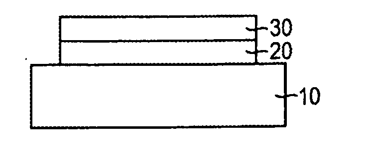
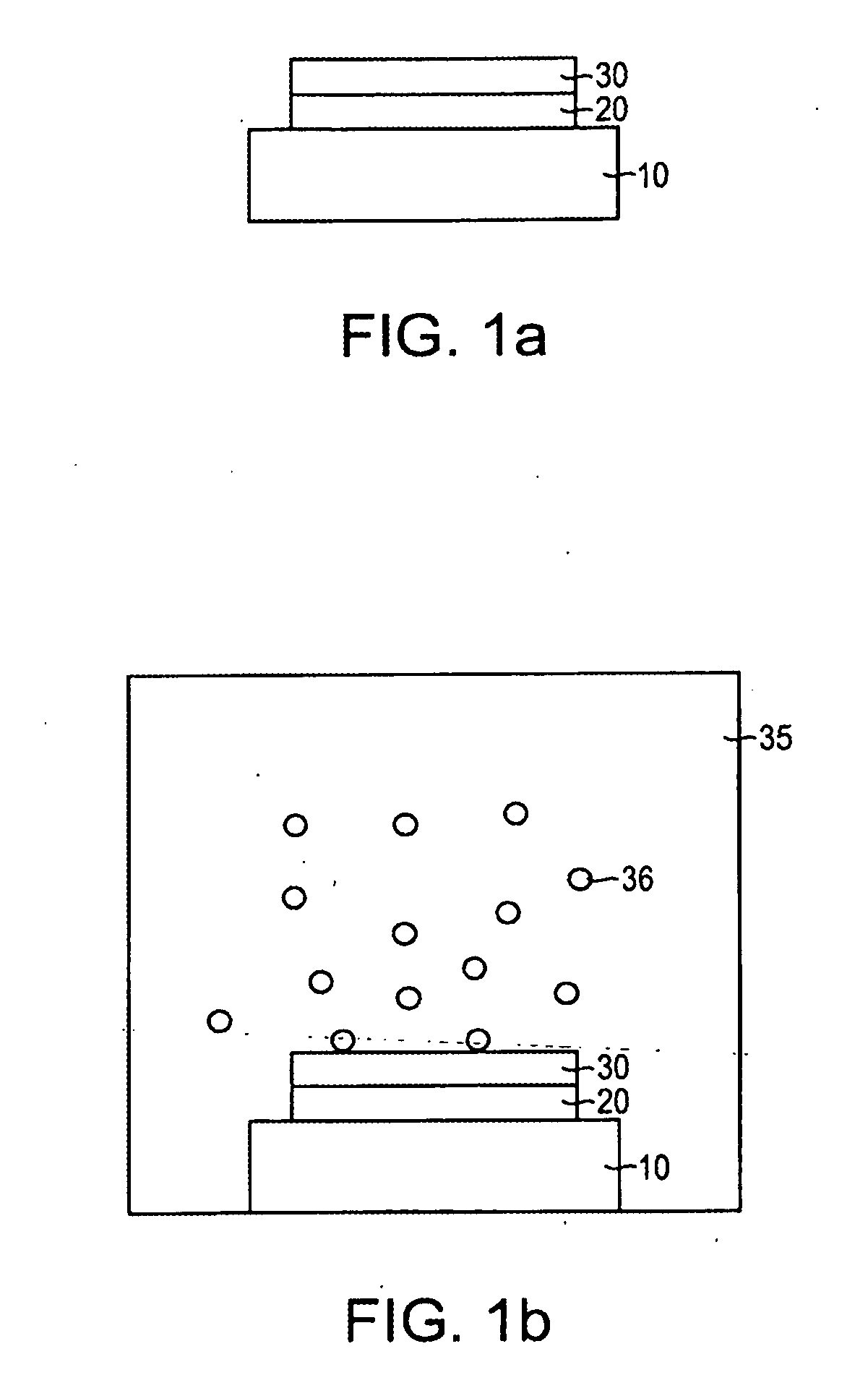
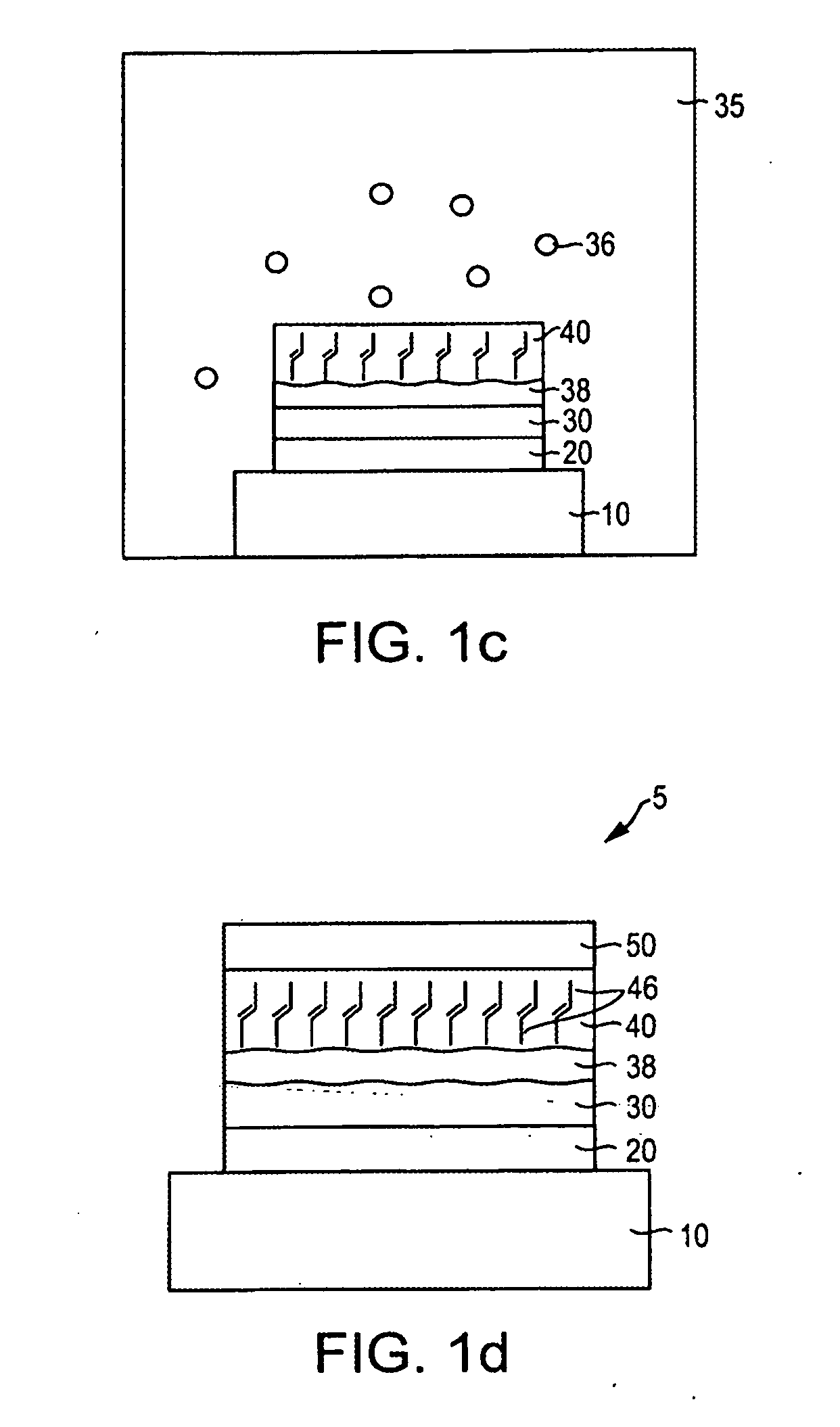
[0024] The present invention provides novel electrical devices and methods of forming such devices. In these devices and methods, an easily formed molecular composite material, such as a polymer, is electrically coupled between two electrodes. The composite material includes mobile ions for electrically switching the memory device. The mobile ions are derived from a source layer during formatio...


PUM


Abstract

A molecular memory cell and methods for forming a molecular memory cell, which allow for easy and inexpensive manufacturing and flexibility in memory system design. Embodiments include a non-volatile molecular memory cell, comprising: a substrate having a conductor, a superionic conductor, a polymer layer over said superionic conductor, a layer of metal ions formed from the superionic conductor and residing between said polymer layer and said superionic conductor, and a second conductor over the polymer layer. Other embodiments include methods for forming a molecular memory cell, wherein a superionic conductor is deposited over a suitable substrate having conductor. A polymeric film is then deposited over the superionic conductor via a living polymerization reaction initiated by the superionic conductor. Furthermore, a layer of excess metal ions from the superionic conductor forms on an upper surface of the superionic conductor. A top conductor is then formed on the polymeric film.

Description

FIELD OF THE INVENTION [0001] The invention relates to the field of random access memory (RAM) devices and resistance devices formed using a resistance variable material. BACKGROUND [0002] Semiconductor Memory devices can generally be categorized as either volatile or non-volatile, depending on their speed and data retention characteristics. Typical volatile memory devices include random access memory (RAM). RAM devices are typically volatile in that stored data is lost once the power source is disconnected or removed. Non-limiting examples of RAM devices include dynamic random access memory (DRAM), synchronous dynamic random access memory (SDRAM) and static random access memory (SRAM). In addition, DRAMs and SDRAMs also typically store data in capacitors which require periodic refreshing to maintain the stored data. [0003] Non-volatile memory devices, such as erasable programmable read only memory (“EPROM”), retain data almost indefinitely (more than ten years) without an external ...

Claims


Application Information

Patent Timeline
Patent Type & Authority Applications(United States)
IPC IPC(8): G11C11/00H01L21/8238
CPCG11C13/0014H01L51/0591G11C2213/11G11C13/0016H10K10/50
Inventor CAMPBELL, KRISTY A.
Owner MICRON TECH INC
Why Eureka
Try Eureka