Manufacturing method of semiconductor device

a manufacturing method and semiconductor technology, applied in the direction of individual semiconductor device testing, semiconductor/solid-state device testing/measurement, instruments, etc., can solve the problems of increasing the time required for setting various conditions and evaluations to be used in the wafer test and the post-process of the prototype wafer, and the time required for the initial prototype to be tested and the time required for the prototype to be tested has not been negligible, etc., and the effect of increasing the cost of the prototyp

Inactive Publication Date: 2005-09-22
TRECENTI TECHNOLOGIES INC
View PDF0 Cites 32 Cited by
  • Summary
  • Abstract
  • Description
  • Claims
  • Application Information

AI Technical Summary

Benefits of technology

[0006] Meanwhile, the lead time from the permission by customers to an offer of an initial prototype has become shorter and shorter recently. So, the time required for setting various conditions and evaluations to be used in the wafer test and the post-process of a wafer for prototype has not been negligible for the reduction of the lead time for shipment of the prototype. In particular, although a large scale integrated circuit (LSI) intended for a specific system such as an application specific IC (ASIC) requires much time for design and development, it tends to be obsolete rapidly and its life cycle is short in some cases. Therefore, what matters is how a cycle time is shortened to make delivery quicker. However, in the above-mentioned methods, after a pre-process of a wafer for prototype is completed through the same pre-process as that in the product manufacturing, conditions and evaluation data required in the wafer test process and the post-process are created by using the wafer for prototype, and also, the debugging of a probe card used in the process subsequent to the pre-process of the prototype wafer and the condition setting and adjustment of the design failure of various assembly devices are performed by using the wafer for prototype. Therefore, the shipment of the prototype is delayed and consequently the shortening of the delivery time of semiconductor devices is prevented.
[0007] An object of the present invention is to provide a technique capable of shortening the delivery time of a semiconductor device.
[0012] That is, the delivery time of semiconductor devices can be shortened because, before providing the first wafer, conditions and evaluation data required in the process subsequent to the pre-process of the first wafer can be created and the debugging of various devices used in the process subsequent to the pre-process of the first wafer and the correction of a design failure can also be performed by using the second wafer.

Problems solved by technology

Meanwhile, the lead time from the permission by customers to an offer of an initial prototype has become shorter and shorter recently.
So, the time required for setting various conditions and evaluations to be used in the wafer test and the post-process of a wafer for prototype has not been negligible for the reduction of the lead time for shipment of the prototype.
In particular, although a large scale integrated circuit (LSI) intended for a specific system such as an application specific IC (ASIC) requires much time for design and development, it tends to be obsolete rapidly and its life cycle is short in some cases.
However, in the above-mentioned methods, after a pre-process of a wafer for prototype is completed through the same pre-process as that in the product manufacturing, conditions and evaluation data required in the wafer test process and the post-process are created by using the wafer for prototype, and also, the debugging of a probe card used in the process subsequent to the pre-process of the prototype wafer and the condition setting and adjustment of the design failure of various assembly devices are performed by using the wafer for prototype.

Method used


Image

  • Manufacturing method of semiconductor device
  • Manufacturing method of semiconductor device
  • Manufacturing method of semiconductor device

Examples


first embodiment

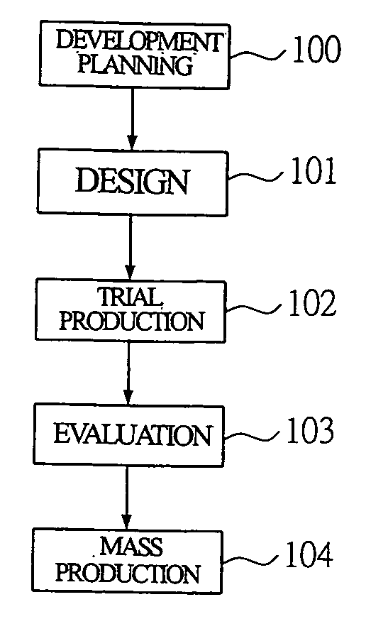
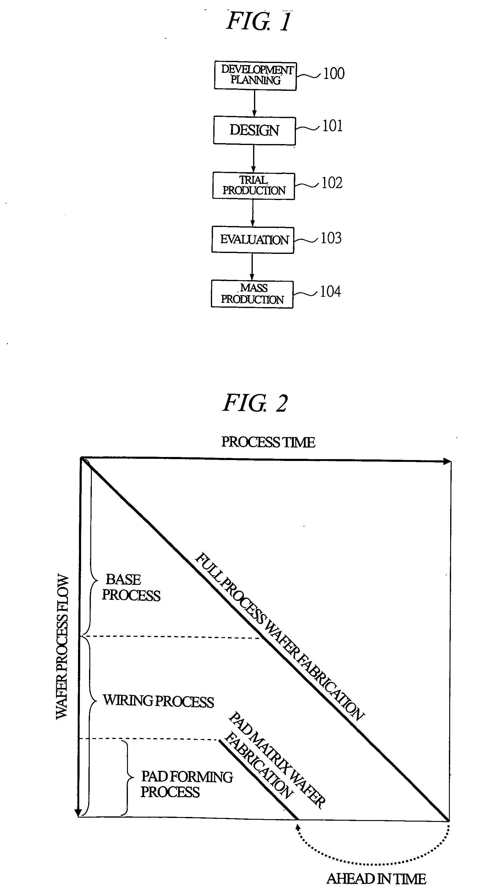
[0058]FIG. 1 shows a production flow chart of the semiconductor device according to a first embodiment.

[0059] First, this flow starts from a development planning 100 of products and moves to a design process 101. In the design process 101, a functional design, logical design, circuit design, device process design, and mask design for integrated circuit are performed in this order. In the functional design, logical design, and circuit design, a computer aided design (CAD) system is used to create data for product design, perform various verifications, and ensure and adjust the functions and performances based on simulation. In the device process design, experiments and data collection are repeated in consideration of a technical level for the mass production of the product (minimum dimensions, device structure, processes, manufacturing devices, production line and others) by using an element unit level and a small-scale Integrated circuit (IC) to determine the conditions. On the bas...

second embodiment

[0107] In a second embodiment, an example of the case where the product chip has a damascene interconnect structure will be described.

[0108]FIG. 35 illustrates a cross-sectional view of a main part of the chip 4a of the prototype wafer 1A. Since the planar configuration of the prototype wafer 1A in the second embodiment is the same as that in the first embodiment, the description thereof is omitted. Also, since the configuration of the product wafer in the second embodiment is the same as that of the prototype wafer 1A to be described in the second embodiment, the description thereof is omitted.

[0109] On the insulating layer 15a, a plurality of insulating layers 38 and 39 are alternately laminated. The insulating layer 38 is made of, for example, silicon nitride and the insulating layer 39 is made of, for example, silicon oxide. The insulating layer 39 can be formed of an insulating material with a dielectric constant lower than that of the silicon oxide. The insulating materials ...

third embodiment

[0113] In the third embodiment, an example of the application in the case where a product chip is manufactured by using a wafer process package (hereinafter referred to as WPP) technique will be described. The WPP technique includes a step of collectively performing a package process at once for a plurality of chips on the wafer formed through the wafer process before dicing the wafer.

[0114] First, an example of manufacturing process of the prototype in the WPP will be described with reference to FIGS. 37 to 41. FIGS. 37 to 41 are explanatory diagrams of manufacturing process of the prototype in the WPP. Since the method for manufacturing the product is the same as that of the prototype, the description thereof is omitted.

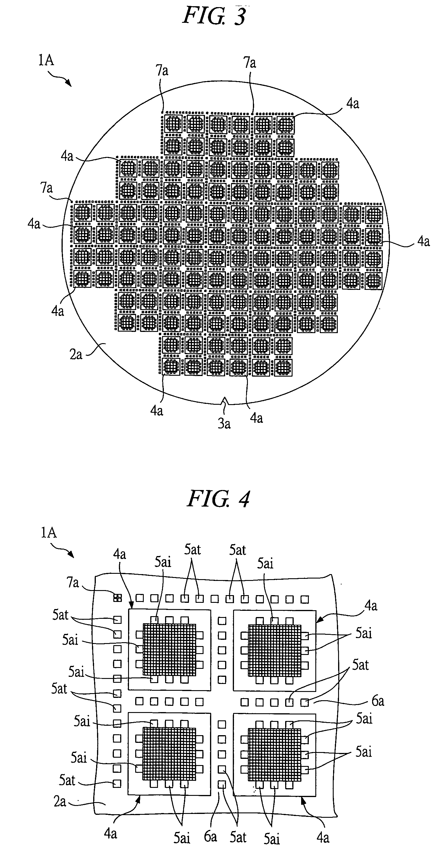
[0115]FIG. 37 is a general plan view showing an example of the prototype wafer 1A after the pre-process. In this example, a plurality of the pads 5ai are arranged along the longitudinal center line of each chip 4a on the main surface of the prototype wafer 1A (a ...


PUM


Abstract

In a trial production process from a design process to an actual manufacturing process of semiconductor devices, a pre-process of a pad matrix wafer with simpler configuration than a prototype wafer is completed before a pre-process of the prototype wafer is completed, and data of conditions and evaluations to be used in a test process and a post-process subsequent to the pre-process of the prototype wafer is created by using the pad matrix wafer. Therefore, the data of conditions and evaluations used in the process subsequent to the pre-process can be prepared and the design modifications of various devices used in the process subsequent to the pre-process can be finished before the post-process of the prototype wafer is started. Therefore, a smooth transition from the pre-process to the subsequent processes of the prototype can be achieved, and the delivery time of semiconductor devices can be shortened.

Description

CROSS-REFERENCE TO RELATED APPLICATION [0001] The present application claims priority from Japanese Patent Application JP 2004-080621 filed on Mar. 19, 2004, the content of which is hereby incorporated by reference into this application. TECHNICAL FIELD OF THE INVENTION [0002] The present invention relates to a technique for manufacturing a semiconductor device. More particularly, it relates to a technique which is effective when applied to the setting of various conditions to be used in the process subsequent to the pre-process in the manufacturing process of a semiconductor device. BACKGROUND OF THE INVENTION [0003] Semiconductor devices are mass-produced and shipped through several steps such as an initial development planning, various design processes, reticle work process, and trial and evaluation process. In the trial and evaluation process, a prototype is produced by using a reticle produced through the reticle work process in a trial production line or a mass-production line...

Claims


Application Information

Patent Timeline
Patent Type & Authority Applications(United States)
IPC IPC(8): H01L21/28G01R31/26H01L21/00H01L21/02H01L21/3205H01L21/66H01L23/52H01L23/544
CPCH01L22/20H01L22/34H01L2924/13091H01L2224/48227H01L2224/48091H01L2924/014H01L2224/02166H01L2224/05554H01L2224/05556H01L2224/0401H01L2224/04042H01L24/05H01L2224/13H01L2924/00014H01L2924/00H01L2224/0392H01L2224/05093H01L2924/12036H01L2924/12041H01L2924/14H01L2924/181
Inventor YAMADA, NAOKIMAKIUCHI, TAKESHI
Owner TRECENTI TECHNOLOGIES INC
Why Eureka
Try Eureka