

Soft pellicle for 157 and 193 nm and method of making same
- Summary
- Abstract
- Description
- Claims
- Application Information
AI Technical Summary
Benefits of technology
Problems solved by technology
Method used
Image

Examples
example 1
Preparation of Soft Pellicles using PTFE
[0059] Cross-linked polytetrafluoroethylene (PTFE) is presented in this example as a solution for soft pellicles for 157 nm and previous lithography generations. This material is created using an extremely thin (<25 micron) PTFE that is heated above its melting temperature and irradiated with a high energy electron beam. Adjustments to the film's, properties are completed by variation of temperature, radiation dose, pressure and gas type. These properties include: film thickness, cross-linking density, film uniformity, and degree of crystalinity.
[0060] The starting material is mounted onto an aluminum frame in a class 100-1000 clean room and then inserted into a chamber, sealed, and then pressurized to 1.1 atmospheres with high-purity argon. The temperature of the chamber may be varied from 20° C.-400° C., but will generally be operated between 320° C. and 385° C. Prior to heating of the chamber, the system is purged with high purity argon (...
example 2
Process Chamber Apparatus
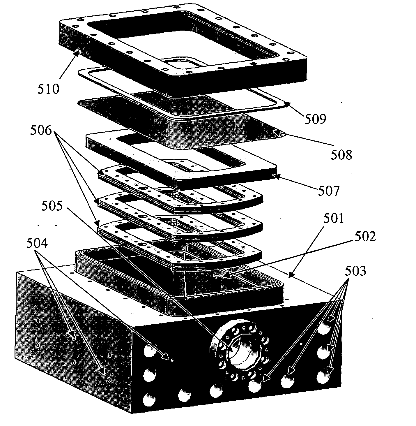
[0067] A process chamber apparatus (or “polymer exposure system” apparatus) was created to allow irradiation and fluorination of perfluorinated polymers in the same chamber. FIG. 5 illustrates an embodiment of the process chamber apparatus. Direct fluorination may be accomplished in the same chamber as shown in FIG. 5, and this chamber allows for the introduction of gasses or vacuum.
[0068] Element 501 (FIG. 5) is the base chamber (e.g., a chamber made of aluminum) in which the electron beam irradiation of the polymer films will occur. The block may be composed of aluminum and, in a preferred embodiment, measures 254 mm×330 mm×150 mm. Element 502 is a supporting rod in the base chamber. In this embodiment, there are two supporting rods and they are composed of aluminum. Element 503 shows cylindrical openings that house 2000W-heating elements that can be connected to a controller for power regulation. In this embodiment, there are ten 2000W heating elements....
example 3
Preparation of Soft Pellicles Using Perfluorinated Polymers
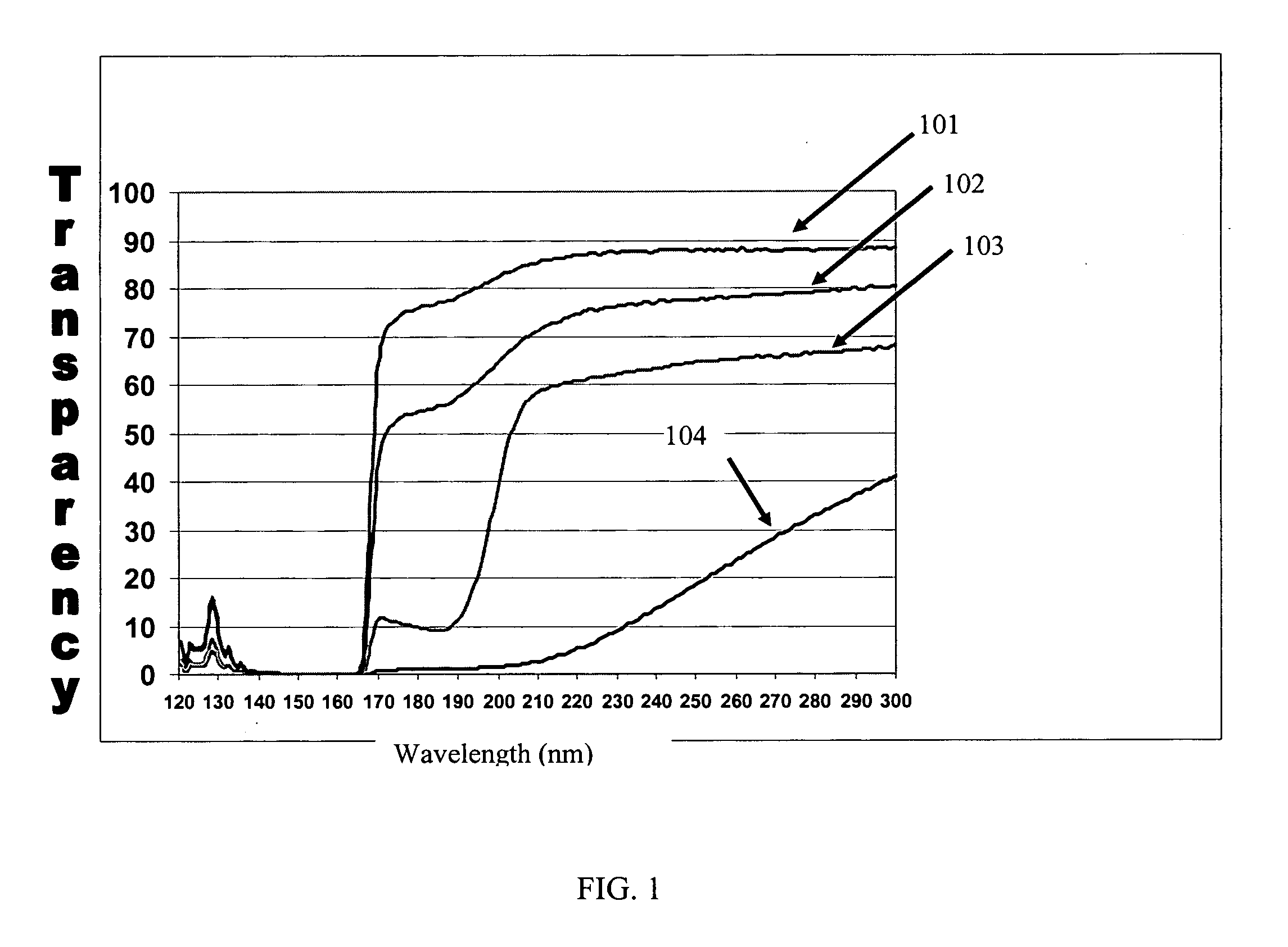
[0077] For several years there has been substantial research into the development of a soft pellicle solution for 157 nm lithography and an improved pellicle for 193 nm lithography. A pellicle is a thin, transparent and passive film that protects the reticle (mask plate) from having particles deposited and thus imaged on to the wafer. Companies with extensive backgrounds in fluoropolymer development have spent years and a large amount of resources in an attempt to meet the requirements for a 157 nm and 193 nm soft pellicles. Materials developed for use as soft pellicles have shown remarkable transparency, however, none of these materials have been able to survive under 157 nm irradiation for any significant time (Feiring et al., 2003; Matsukura et al., 2002). Materials for 193 nm lithography are available but show shorter lifetimes than expected and sometimes have problems such as particle production. Research conducted ove...
PUM
 Abstract
Description
Claims
Application Information