Semiconductor device and manufacturing method thereof

a technology of semiconductor devices and semiconductors, applied in semiconductor devices, semiconductor/solid-state device details, electrical apparatus, etc., can solve problems such as junction leakage current generation, various problems, and introduction of metal contamination into side surfaces, so as to prevent characteristic deterioration, reduce the concentration of contaminating metals, and prevent characteristic deterioration

Inactive Publication Date: 2005-09-29
ELPIDA MEMORY INC
View PDF5 Cites 22 Cited by
  • Summary
  • Abstract
  • Description
  • Claims
  • Application Information

AI Technical Summary

Benefits of technology

[0012] An object of the present invention is to resolve these problems and provide a semiconductor device and a manufacturing method thereof which can prevent characteristic deterioration due to metallic contamination which occurs during backside grinding, dicing and package assembly.
[0013] In the present invention, a thermal treatment is applied to a backside grinding damage layer or a dicing damage layer in an atmosphere containing an impurit

Problems solved by technology

Moreover, in the subsequent dicing process, dicing damages, which are similar to grinding damages, are introduced into the side surfaces of chips and metallic contamination is also introduced into the side surfaces of the chips.
As described above, once a contaminating metal reaches an electronic device on a main surface of a substrate, various problems become apparent.
For example, when a contaminating metal reaches the depletion layer of a source/drain junction, it leads to the formation of surface state and thus causes the generation of Junction leakage current.
Furthermore, if a contaminating metal reaches a gate insulating film, insulating film leakage current increases.
Because of such increases in the leakage current, characteristics of an electronic device are deteriorated.
The above-mentioned problem has been incr

Method used


Image

  • Semiconductor device and manufacturing method thereof
  • Semiconductor device and manufacturing method thereof
  • Semiconductor device and manufacturing method thereof

Examples


embodiment 1

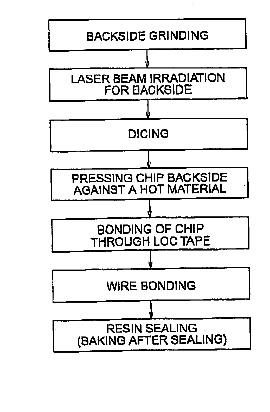
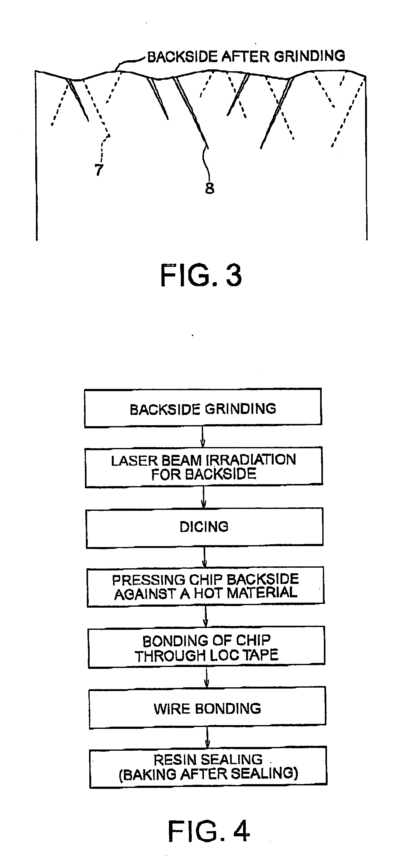
[0031] Embodiments of the present invention are detailed using TSOP assembly of a semiconductor device shown in FIGS. 4 to 11 as examples. An is assembly flowchart of the present invention has additional processes of laser beam irradiation for the backside of a wafer and pressing a hot material to a chip's backside.

[0032] First of all, as shown in the assembly flowchart of FIG. 4, the surface of a silicon wafer, on which semiconductor devices have been fabricated in a normal method, was protected with a protection sheet, and the backside of the wafer was grinded. During this grinding process, the first rough grinding was performed at roughness of about #300 until the wafer thickness becomes about between 750 μm and 300 μm, and finishing grinding was then performed at roughness of about #2000 until the wafer thickness becomes 280 μm. Thereafter, the protection sheet on the surface is removed and washed with water in order to remove dusts attached to the grinded surface during the gr...

embodiment 2

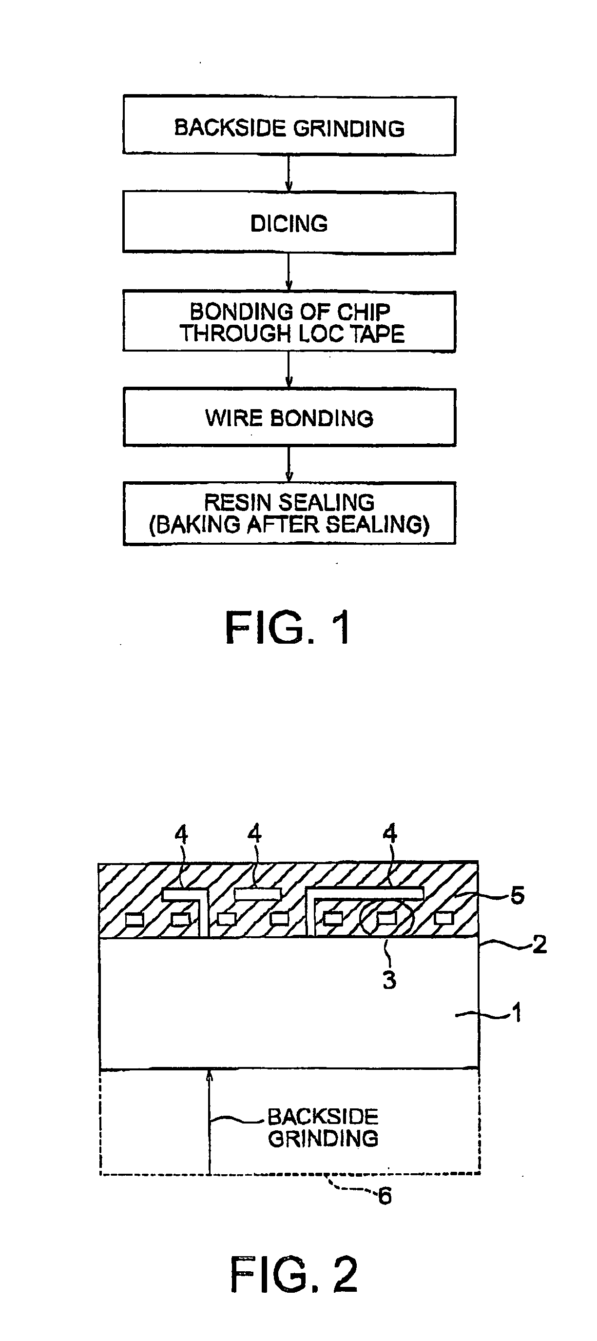
[0051] Next, embodiment 2 in the present invention is detailed using FBGA assembly of a semiconductor device shown in FIGS. 12 to 14 as an example.

[0052] First of all, as shown in the assembly flowchart of FIG. 12, the surface of a silicon wafer on which semiconductor devices are fabricated in a normal method, was protected by a protection sheet, and the backside of the wafer was grinded in that state. During this grinding process, the first rough grinding is performed at roughness of about #300 until the thickness of the wafer becomes about 750 μm and 200 μm, and finishing grinding was then performed at roughness of about #2000 until the thickness of the wafer becomes 180 μm. Here, a comparison is made among a case of grinding using a normal backside grinder, and the following cases in the present invention: [0053] a case (d) where the backside is grinded with copper-contamination-free transfer system, grinding blade and grinding water; [0054] a case (e) where the final grinding i...

embodiment 3

[0060] Next, embodiment 3 of the present invention is detailed. In this Example, the gettering layer described in embodiment 1 was formed by a plasma treatment.

[0061] In the flowchart of FIG. 15, similarly to embodiment 1, a first gettering layer was formed on the backside of a wafer by a first plasma treatment after backside of the wafer was grinded, and then a second gettering layer was formed by a second plasma treatment after the wafer is diced. Both the first and second plasma treatments are carried out in a plasma atmosphere containing an impurity. These plasma treatments were performed, for example, using a plasma device, with plasma power of 2 KW, at substrate temperature of 150 degrees centigrade, using diluent gas containing oxygen as an impurity, at pressure of 1 Torr, and for treatment time of 60 seconds. Processes of backside grinding, dicing, bonding chips to LOC tape, wire bonding, and resin sealing are the same as those of embodiment 1 and descriptions thereof are t...


PUM


Abstract

In manufacturing a semiconductor device, the first gettering layer is formed on the backside of a wafer, and the second gettering layers are then formed on the backside and side surfaces of a chip, allowing these gettering layers to serve as trapping sites against metallic contamination that generated after backside grinding in assembly processes.

Description

[0001] This application claims priority to prior application JP 2004-88308, the disclosure of which is incorporated herein by reference. BACKGROUND OF THE INVENTION [0002] 1. Field of the Invention [0003] The present invention relates to a semiconductor device and a manufacturing method thereof and, particularly, to a semiconductor device and a manufacturing method thereof which can prevent characteristic deterioration due to metallic contamination which occurs in a backside grinding process and a package assembly process performed after formation of desired devices, wiring, and insulating film on a main surface of a semiconductor substrate. [0004] 2. Description of the Related Art [0005] A conventional semiconductor device is fabricated as follows, in accordance with a process flowchart shown in FIG. 1, electronic devices 3, wiring 4, an interlayer Insulating film 5, and the like, are formed on a surface of a silicon substrate 1. Thereafter a substrate's backside 6 is grinded so th...

Claims


Application Information

Patent Timeline
IPC IPC(8): H01L21/322H01L21/02H01L21/302H01L21/304H01L21/461H01L21/50
CPCH01L21/3221H01L21/304H01L21/322
Inventor OYU, KIYONORIOKONOGI, KENSUKEKOBAYASHI, HIROTAKAHAMADA, KOJI
Owner ELPIDA MEMORY INC
Why Eureka
Try Eureka