

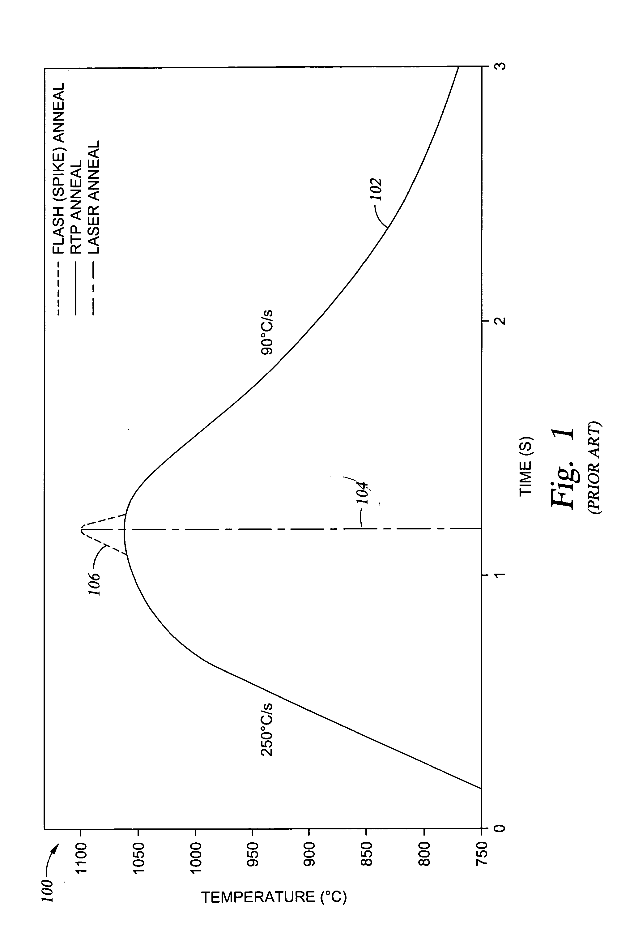
Thermal flux processing by scanning a focused line beam
a technology of focused line beam and thermal flux, which is applied in the direction of solid-state diffusion coating, manufacturing tools, instruments, etc., can solve the problems of increasing increasing the difficulty of adjusting the radiated power requirement, so as to reduce the total radiated power requirement and simplify the control of the apparatus
- Summary
- Abstract
- Description
- Claims
- Application Information
AI Technical Summary
Benefits of technology
Problems solved by technology
Method used
Image

Examples
Embodiment Construction
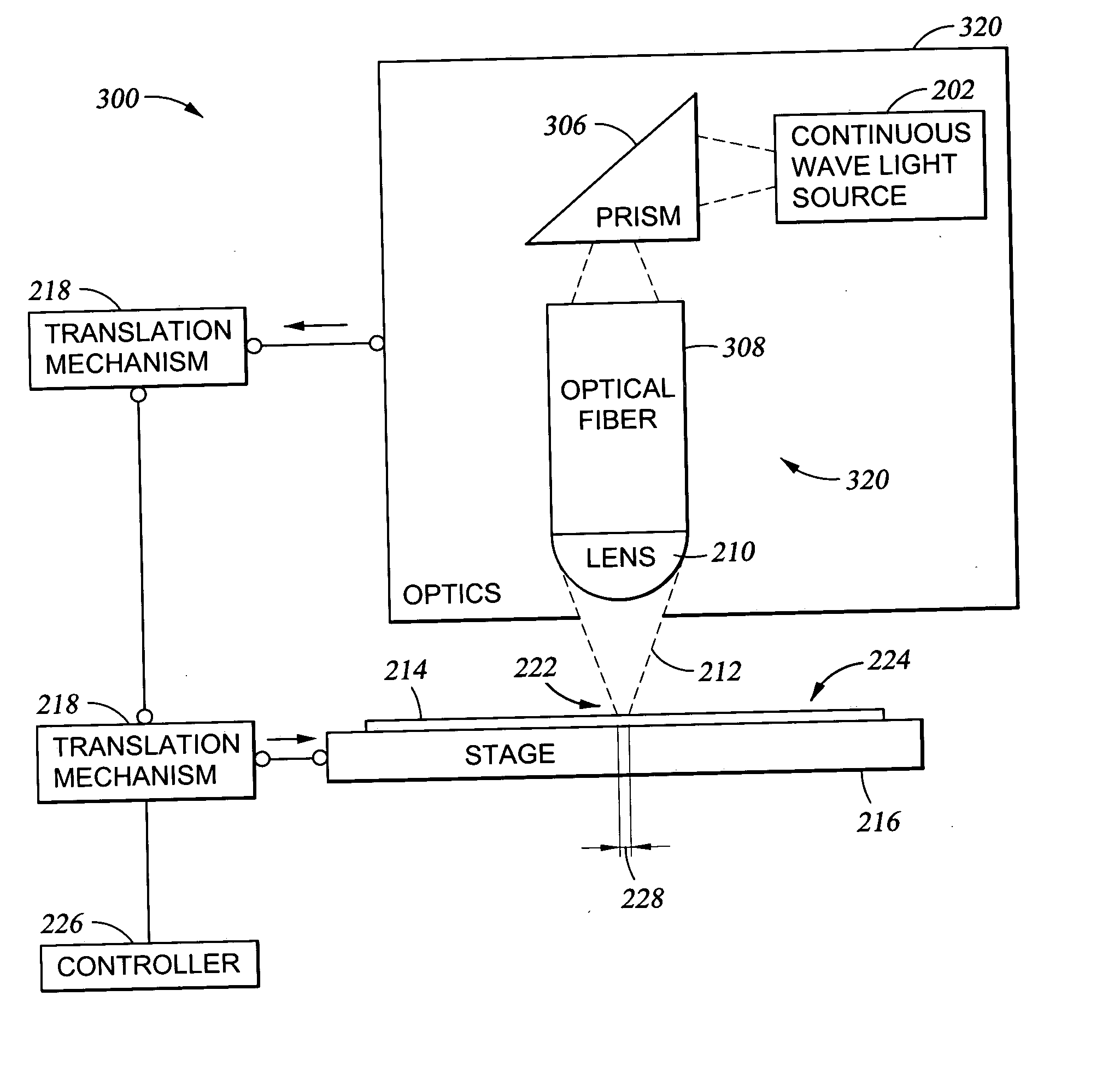
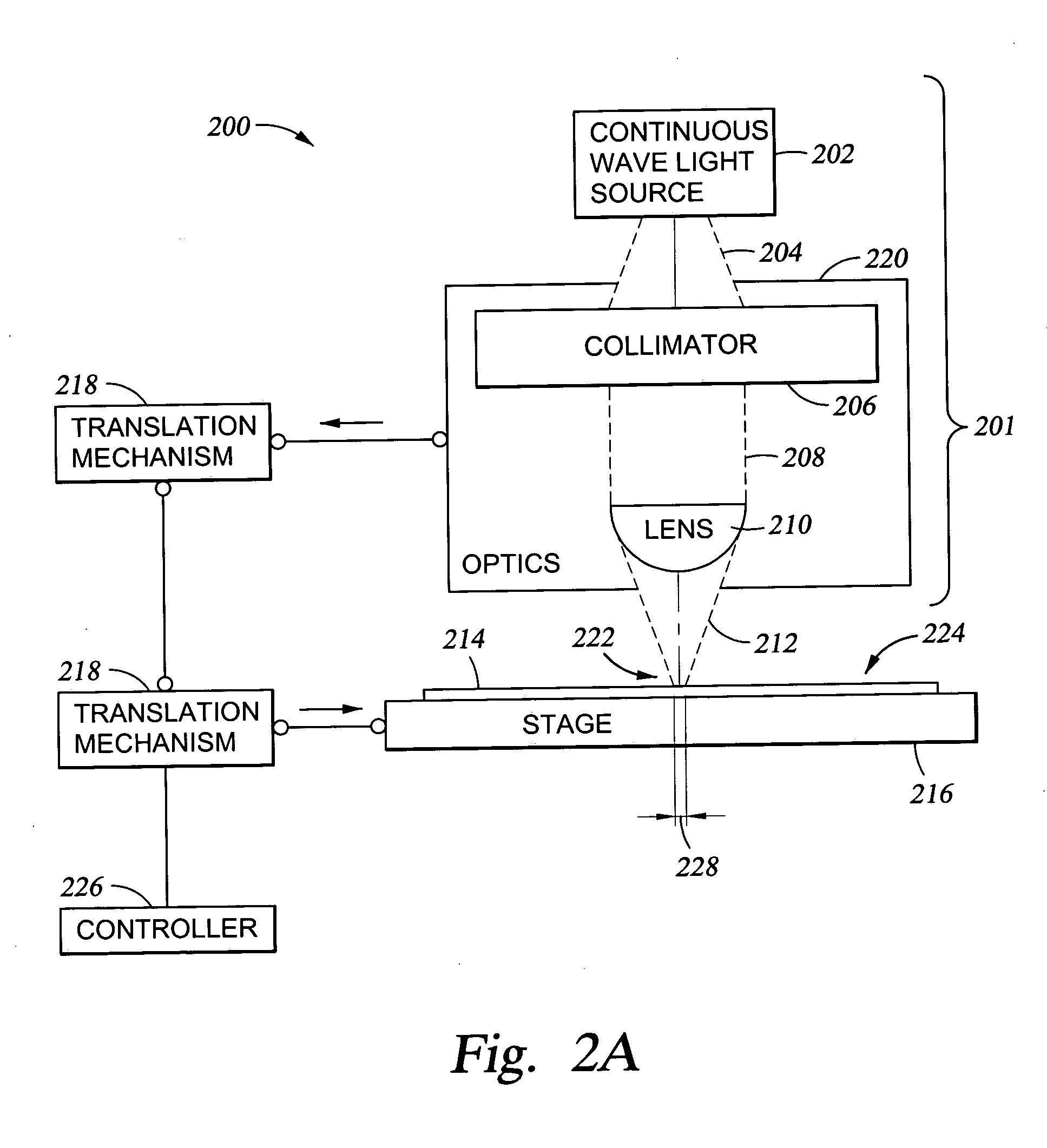
[0071]FIG. 2A is a diagrammatic side view of an apparatus 200 for thermally processing a substrate, according to an embodiment of the invention. Thermally processing a substrate means conducting any thermal process that requires the characteristics of the invention described below. Exemplary embodiments of such a thermal process include thermal annealing of substrates or thermal processes used in chemical vapor ceposition (CVD), both of which will be described throughout the remainder of the Figures.
[0072] The apparatus 200 comprises a continuous wave electromagnetic radiation module 201, a stage 216 configured to receive a substrate 214 thereon, and a translation mechanism 218. The continuous wave electromagnetic radiation module 201 comprises a continuous wave electromagnetic radiation source 202 and focusing optics 220 disposed between the continuous wave electromagnetic radiation source 202 and the stage 216.
[0073] In a preferred embodiment, the substrate 214 is any suitable s...
PUM
| Property | Measurement | Unit |
|---|---|---|
| Height | aaaaa | aaaaa |
| Symmetric field theory | aaaaa | aaaaa |
| Power density | aaaaa | aaaaa |
Abstract
Description
Claims
Application Information