Semiconductor device

a technology of semiconductor devices and thin-film resistors, which is applied in the direction of semiconductor devices, solid-state devices, basic electric elements, etc., can solve the problems of difficult patterning of refractory metal films by dry etching techniques, difficult to prevent connecting holes b, and difficult to prevent the penetration of connecting holes b, etc., to achieve accurate resistance values, reduce the variation of contact resistance between metal thin-film resistors and metal wiring patterns, and improve the effect of yield

Inactive Publication Date: 2005-10-06
RICOH KK
View PDF2 Cites 18 Cited by
  • Summary
  • Abstract
  • Description
  • Claims
  • Application Information

AI Technical Summary

Benefits of technology

[0072] In the second embodiment with the sidewalls, the wiring pattern is formed with a metal material pattern and a refractory metal film that is formed at least on the upper surface of the metal material pattern. In this manner, the refractory metal film can be interposed between the metal thin-film resistor and the wiring pattern. Accordingly, the variation in the contact resistance between the metal thin-film resistor and the metal wiring pattern can be reduced. Thus, more accurate resistance values can be obtained, and higher yield can be achieved. In a structure in which the metal thin-film resistor is in contact with a metal material, the contact resistance greatly varies when thermal treatment is performed at a relatively low temperature of 300° C. to 400° C. With the above described structure, such a problem can also be eliminated.
[0073] In the second embodiment with the sidewalls, the wiring pattern is formed with a polysilicon pattern and a refractory metal film that is formed at least on the upper surface of the polysilicon pattern. In this manner, the refractory metal film can be interposed between the metal thin-film resistor and the wiring pattern. Accordingly, the variation in the contact resistance between the metal thin-film resistor and the wiring pattern can be reduced. Thus, more accurate resistance values can be obtained, and higher yield can be achieved.
[0074] Any of the semiconductor devices of the first and second embodiments may further include a metal nitride film that covers the upper surface of the metal thin-film resistor, while a metal oxide film is not formed between the upper surface of the metal thin-film resistor and the metal nitride film. In this manner, the upper surface of the metal thin-film resistor cannot be oxidized. Thus, the resistance of the metal thin-film resistor can be stabilized, and more accurate resistance values can be obtained.
[0075] In a semiconductor device equipped with a dividing resistive circuit that obtains a voltage output through a dividing process using two or more resistance elements, and

Problems solved by technology

If the metal thin-film resistor 101 is thinner than 1000 Å, however, it is difficult to prevent the connecting holes 107 from penetrating the metal thin-film resistor 101.
Since the refractory metal film exists immediately above the

Method used


Image

  • Semiconductor device
  • Semiconductor device
  • Semiconductor device

Examples


first embodiment

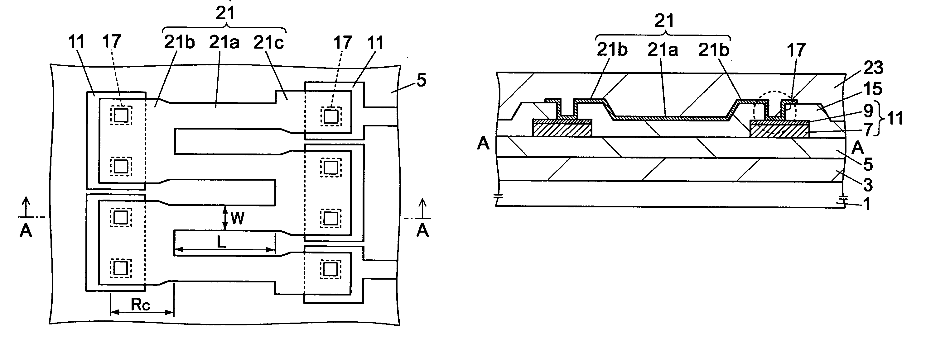
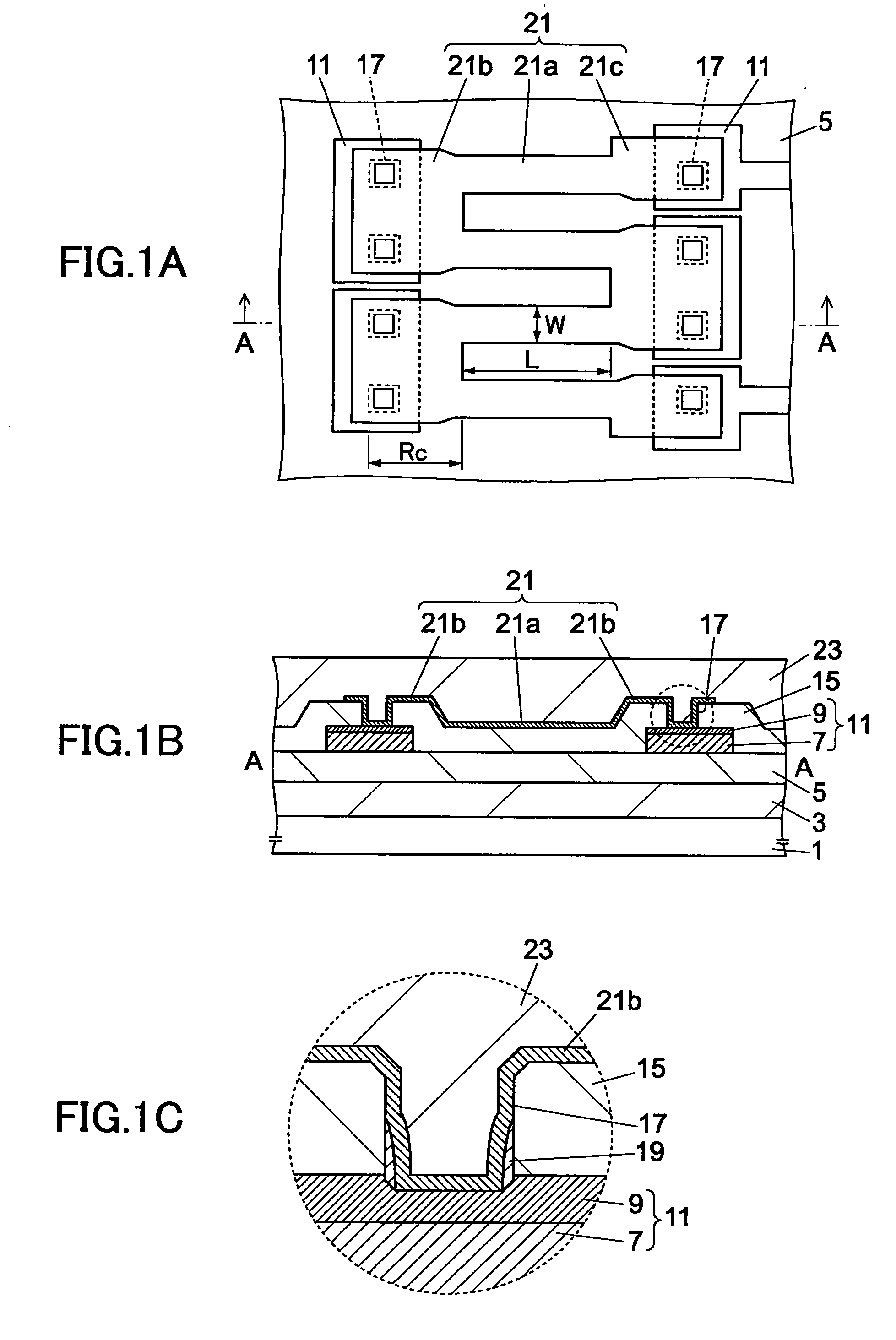
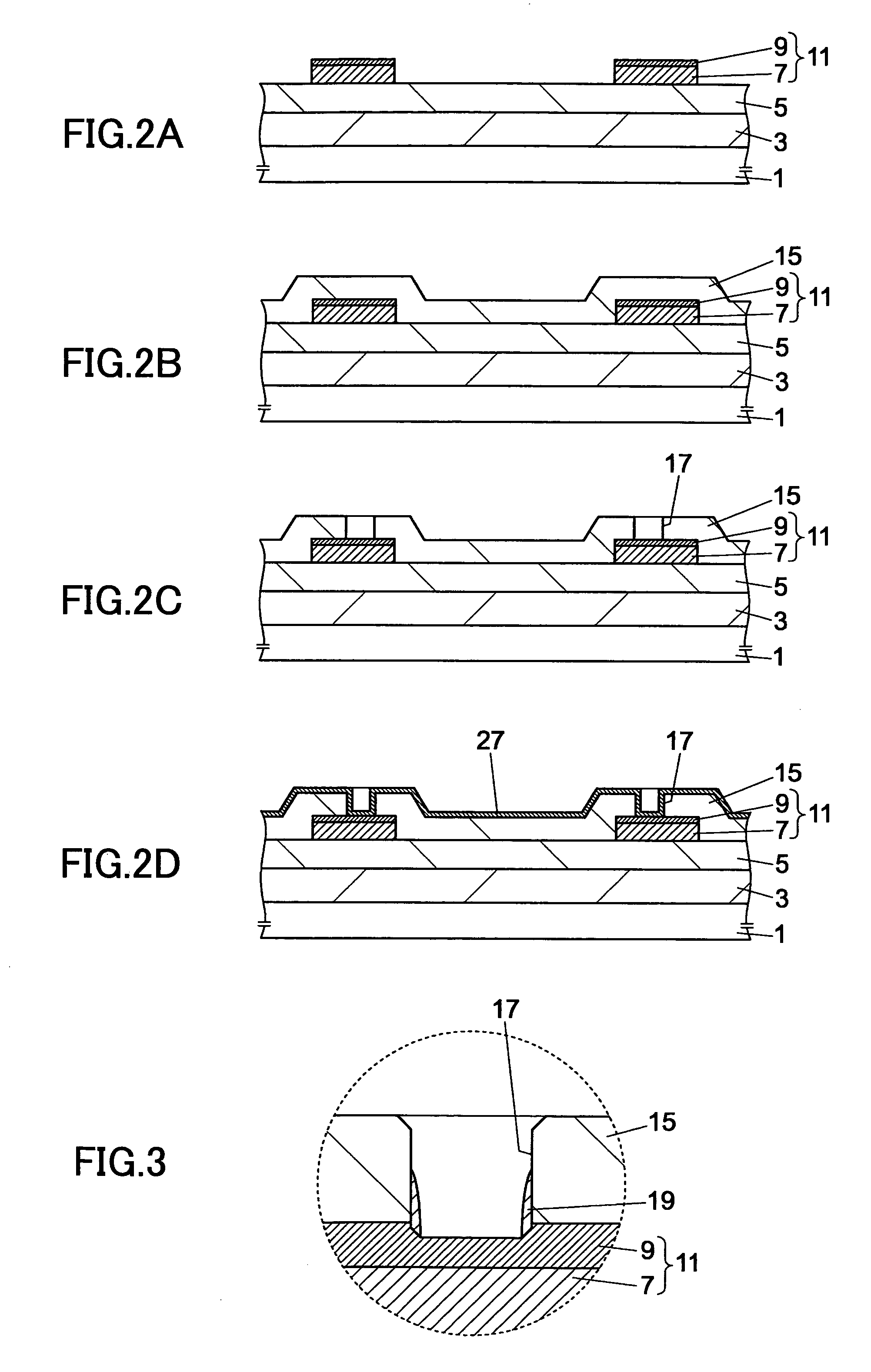
[0139]FIGS. 1A through 1C illustrate the present invention. FIG. 1A is a plan view of a part of the region for forming metal thin-film resistors. FIG. 1B is a cross-sectional view, taken along the line A-A of FIG. 1A. FIG. 1C is an enlarged cross-sectional view of the portion circled by a broken line in FIG. 1B. In FIG. 1A, the base insulating film and the passivation film are not shown. In the embodiments described below, a transistor device and a capacitive device are formed on the same substrate, but those devices are not shown in the drawings.

[0140] A device isolating oxide film 3 is formed on a silicon substrate 1. An interlayer insulating film (a lower-layer insulating film) 5 that is formed with a BPSG (borophospho silicate glass) film or a PSG (phospho silicate glass) film is formed on the silicon substrate 1 including the region for forming the device isolating oxide film 3. Metal wiring patterns 11 that are formed with metal material patterns 7 and refractory metal films 9...

second embodiment

[0256]FIGS. 12A through 12C illustrate an example structure of the present invention. FIG. 12A is a plan view of a part of the formation region of a metal thin-film resistor. FIG. 12B is a cross-sectional view of the structure, taken along the line C-C of FIG. 12A. FIG. 12C is an enlarged cross-sectional view of the portion surrounded by the broken line of FIG. 12B. In FIG. 12A, the passivation film is not shown. In FIGS. 12A through 12C, the components having the same functions as those of the foregoing examples are denoted by the same reference numerals as in the foregoing examples, and explanation of them is omitted herein.

[0257] A device isolating oxide film 3 is formed on a silicon substrate 1. An interlayer insulating film 5 is formed on the silicon substrate 1 including the formation region of the device isolating oxide film 3. In this example, the interlayer insulating film 5 forms a base insulating film for a CrSi thin-film resistor 21.

[0258] Metal wiring patterns 11 forme...


PUM


Abstract

A semiconductor device is provided that includes: a base insulating film; a metal thin-film resistor that is provided on the base insulating film; a lower-layer insulating film that is formed under the base insulating film; and a wiring pattern that is formed on the lower-layer insulating film. In this semiconductor device, the base insulating film is formed on the lower-layer insulating film and the wiring pattern, and connecting holes are formed in the base insulating film located on the wiring patterns. The metal thin-film resistor has at least two belt-like portions and a return portion that continues to the belt-like portions. The belt-like portions are located at a distance from the region on the wiring pattern. The return portion connects at least two belt-like portions in a position at a distance from the region on the wiring pattern. The return portion is formed in a connecting hole via the region on the wiring pattern.

Description

BACKGROUND OF THE INVENTION [0001] 1. Field of the Invention [0002] The present invention relates to a semiconductor device, and, more particularly, to a semiconductor device that has a metal thin-film resistor on a base insulating film. [0003] 2. Description of the Related Art [0004] In analog integrated circuits, resistor devices are often employed as essential components. In recent years, attention has been drawn to resistors that are formed with metal thin films (hereinafter referred to as metal thin-film resistors), as the resistance of a metal thin-film resistor has low temperature dependency (or a small TCR). The materials for the metal thin-film resistors include chromium silicon (CrSi), nickel chromium (NiCr), tantalum nitrogen (TaN), chromium silicide (CrSi2), chromium silicide nitride (CrSiN) and chromium silicon oxide (CrSiO). [0005] To satisfy the requirement for higher integrated analog circuits in a semiconductor device having metal thin-film resistors, each metal thi...

Claims


Application Information

Patent Timeline
IPC IPC(8): H01L21/768H01C7/00H01C17/075H01L21/822H01L23/525H01L27/04H01L27/08H01L29/00
CPCH01C7/006H01C17/075H01L23/5258H01L27/0802H01L2924/0002H01L2924/00
Inventor WATANABE, HIROFUMI
Owner RICOH KK
Why Eureka
Try Eureka