Glass molding die, renewal method thereof, and glass fabricated by the molding die
a technology of glass molding and molding die, which is applied in the field of mold molding die and the renewal method thereof, can solve the problems of difficult and time-consuming renewal process, rapid damage to the chromium layer of diamond tools, so as to improve the renewability and shorten the renewal time
- Summary
- Abstract
- Description
- Claims
- Application Information
AI Technical Summary
Benefits of technology
Problems solved by technology
Method used
Image
Examples
example 1
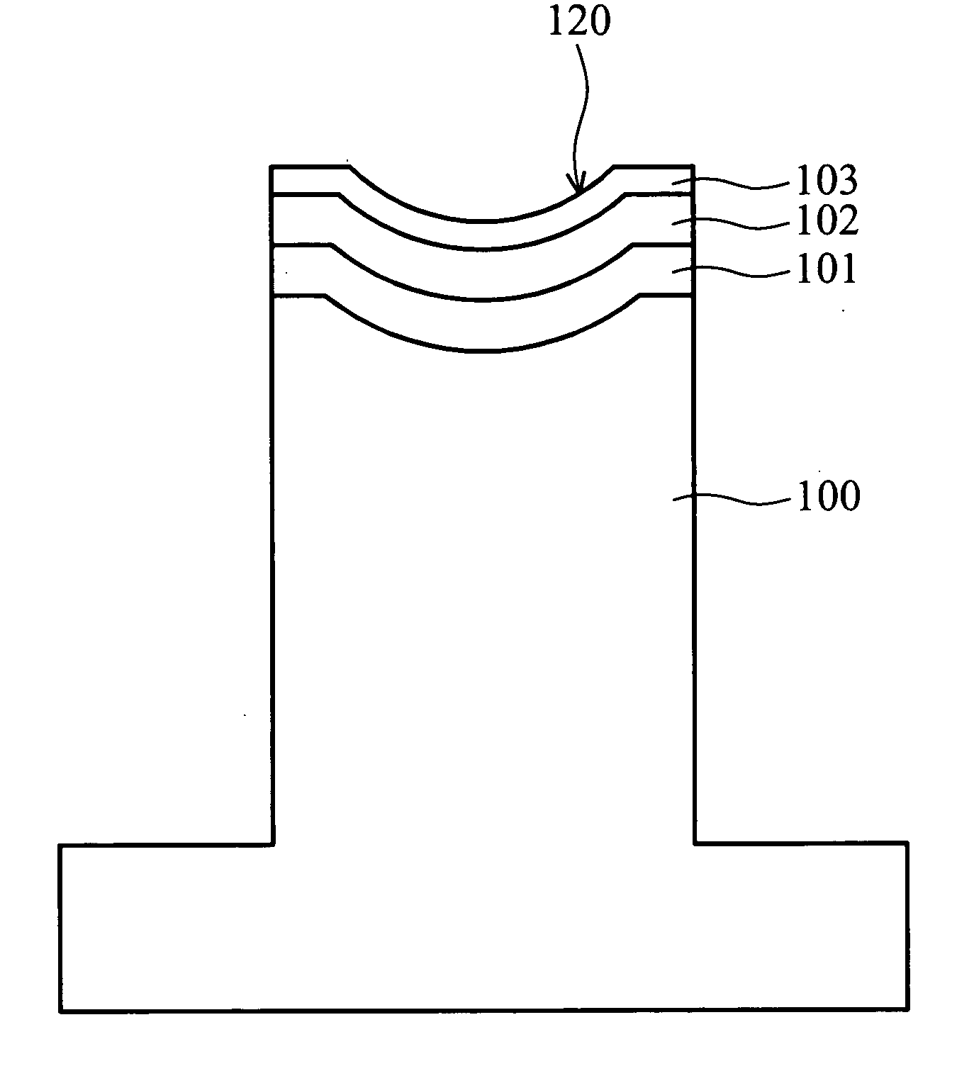
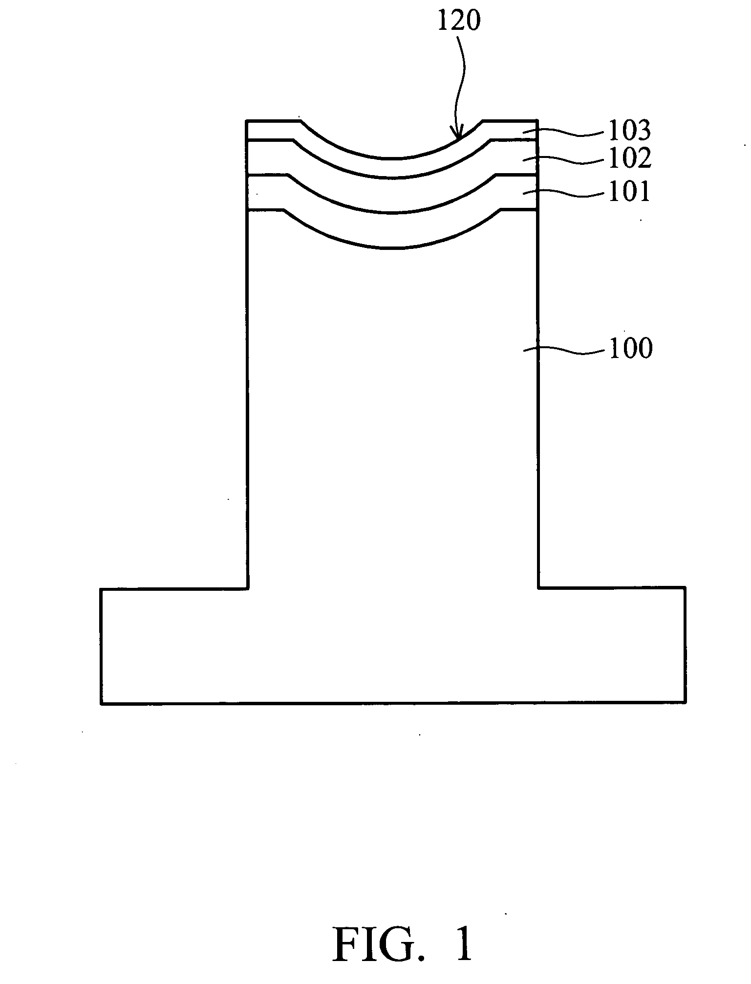
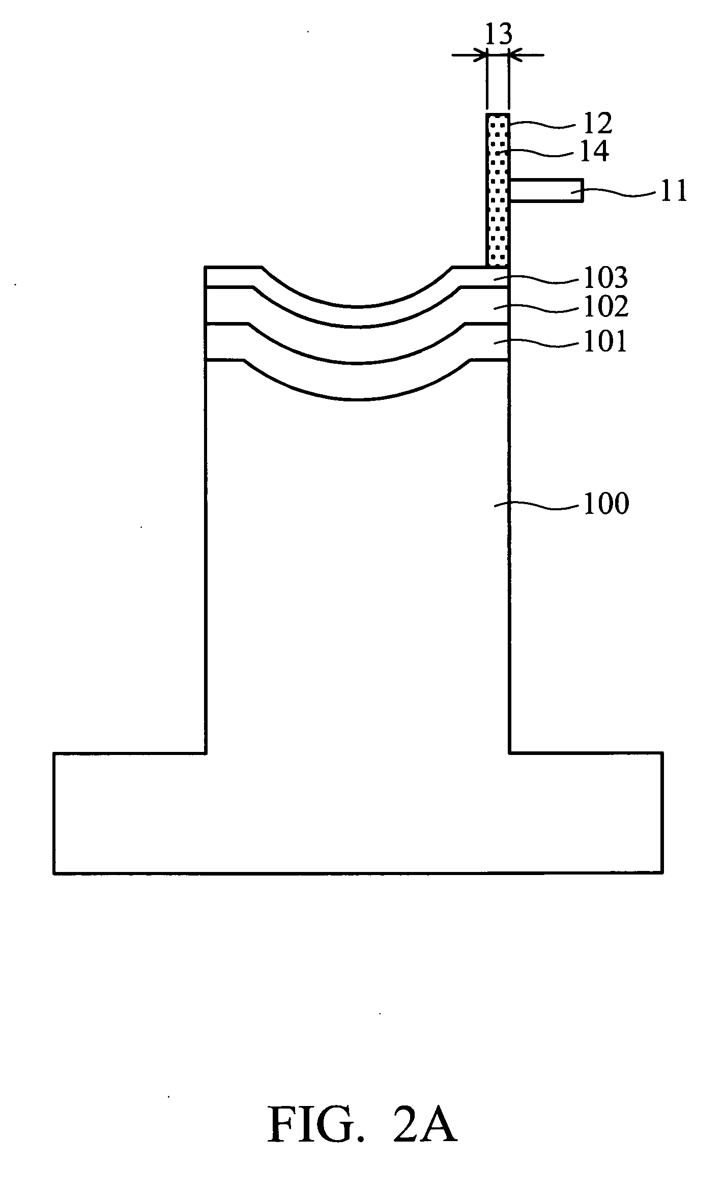
[0036] A tungsten carbide substrate 100 was machined to create an approximately spherical surface, followed by formation of a nickel-phosphorous alloy layer 101, with low phosphorous content (approximately 3 wt %) and of approximately 30 μm thickness, using electroless plating. The nickel-phosphorous alloy layer 101 was ground to achieve a desired surface accuracy and roughness, followed by sequential formation of a Pt—Ir—Ni layer of approximately 0.1 μm thick and Pt—Ir layer of approximately 0.3 μm thick respectively acting as an intermediate layer 102 and passivation film 103. Thus, a molding die of the present invention was completed.
[0037] The molding die then served in a glass molding process. When the roughness (Rms) of the molding die exceeded 20 Å, the intermediate layer 102 and passivation film 103 were removed by grinding. A ratio of wear rates of the nickel-phosphorous alloy layer 101, intermediate layer 102, and passivation film 103 of described compositions was approxi...
example 2
[0038] A tungsten carbide substrate 100 was machined to create an approximately spherical surface, followed by formation of a nickel-phosphorous alloy layer 101, with high phosphorous content (approximately 12 wt %) and of approximately 50 μm thick, using electroless plating. The nickel-phosphorous alloy layer 101 was cut to achieve a desired surface accuracy and roughness, followed by sequential formation of a Pt—Ir—Ni layer of approximately 0.1 μm thickness and Pt—Ir layer of approximately 0.3 μm thickness respectively acting as an intermediate layer 102 and passivation film 103. Thus, a molding die of the present invention was completed.
[0039] The molding die then served in a glass molding process. When the roughness (Rms) of the molding die exceeded 20 Å, the intermediate layer 102 and passivation film 103 were removed by grinding. A ratio of wear rates of the nickel-phosphorous alloy layer 101, intermediate layer 102, and passivation film 103 of described compositions was appr...
example 3
[0040] A tungsten carbide substrate 100 was machined to create an approximately spherical surface, followed by formation of a tungsten containing nickel-phosphorous alloy layer 101, with high phosphorous content (approximately 15 wt % of phosphorous and 7 wt % of tungsten) and of approximately 50 μm thickness, using electroless plating. The nickel-phosphorous alloy layer 101 was diamond-turned to achieve a desired surface accuracy and roughness, followed by sequential formation of a Pt—Ir—Ni layer of approximately 0.1 μm thickness and Pt—Ir layer of approximately 0.3 μm thickness respectively acting as an intermediate layer 102 and passivation film 103. Thus, a molding die of the present invention was completed.
[0041] The molding die then served in a glass molding process. When the roughness (Rms) of the molding die exceeded 20 Å, the intermediate layer 102 and passivation film 103 were removed by grinding. A ratio of wear rates of the nickel-phosphorous alloy layer 101, intermedia...
PUM
| Property | Measurement | Unit |
|---|---|---|
| Thickness | aaaaa | aaaaa |
| Thickness | aaaaa | aaaaa |
| Thickness | aaaaa | aaaaa |
Abstract
Description
Claims
Application Information


