Ultraviolet group III-nitride-based quantum well laser diodes

a quantum well and laser diode technology, applied in the field of semiconductor laser diodes, can solve the problems of polarization effects, uneven carrier distribution, and unique problems of gan materials systems in the realization of uv lasers

Inactive Publication Date: 2005-10-13
PALO ALTO RES CENT INC
View PDF7 Cites 66 Cited by
  • Summary
  • Abstract
  • Description
  • Claims
  • Application Information

AI Technical Summary

Benefits of technology

[0013] One aspect of the design of such single quantum well or coupled quantum well devices, is the design of a carrier confinement structure, to contain the carriers within the active region, while not contributing to the loss in the device.
[0022] In various exemplary embodiments according to this invention, a single quantum well or coupled quantum well laser diode active region is described which uses (indium) aluminum gallium nitride carrier confinement layers adjacent to the indium gallium nitride single or coupled quantum well to provide the necessary electron and hole confinement. The electron and hole confinement layers are partially doped with silicon or magnesium, to supply sufficient carrier confinement for electrons and holes. In various exemplary embodiments according to this invention, a portion of the confinement layers directly adjacent to the quantum well are left undoped, to reduce impurity scattering and prevent structural degradation of the single quantum well laser diode. In various exemplary embodiments according to this invention, the undoped spacer layers increase the gain and reduce the threshold current of the single or coupled quantum well laser diode.

Problems solved by technology

However, GaN materials systems present unique problems in terms of realizing a UV laser.
Polarization effects are particularly detrimental for In(Al)GaN / (In)AlGaN multi-quantum wells, where the fields cause not only uneven carrier distribution within but also uneven carrier distribution between the quantum wells.
However the high barriers will also prevent carriers from moving easily between quantum wells and therefore make it difficult to achieve a even distribution of carriers between quantum wells.
Unevenly distributed carriers lead to uneven gain, which results in higher threshold current densities and lower quantum efficiencies.
In this case, the carrier distributions can be so non-uniform that one or more of the quantum wells in the active region is below the transparency threshold, which can even quench lasing.

Method used


Image

  • Ultraviolet group III-nitride-based quantum well laser diodes
  • Ultraviolet group III-nitride-based quantum well laser diodes
  • Ultraviolet group III-nitride-based quantum well laser diodes

Examples


Embodiment Construction

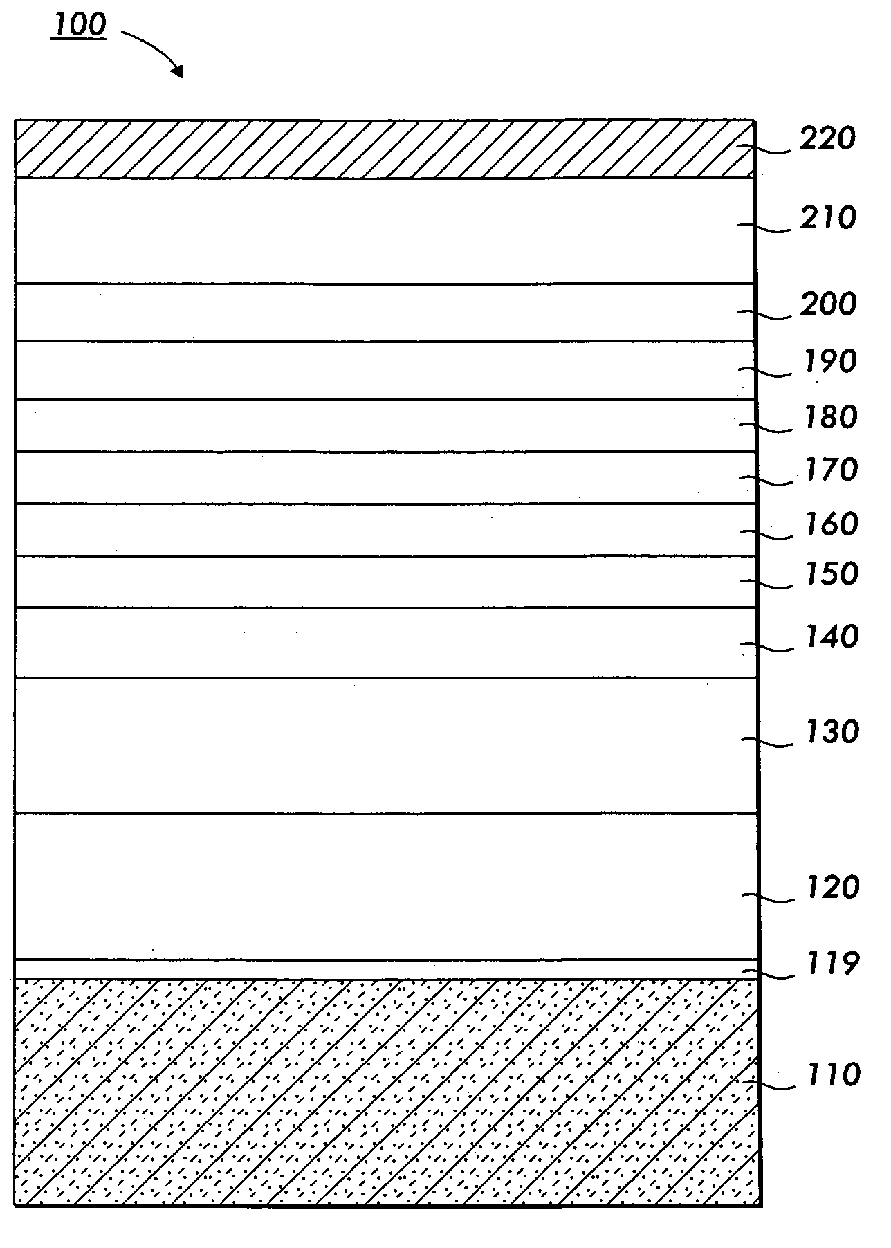
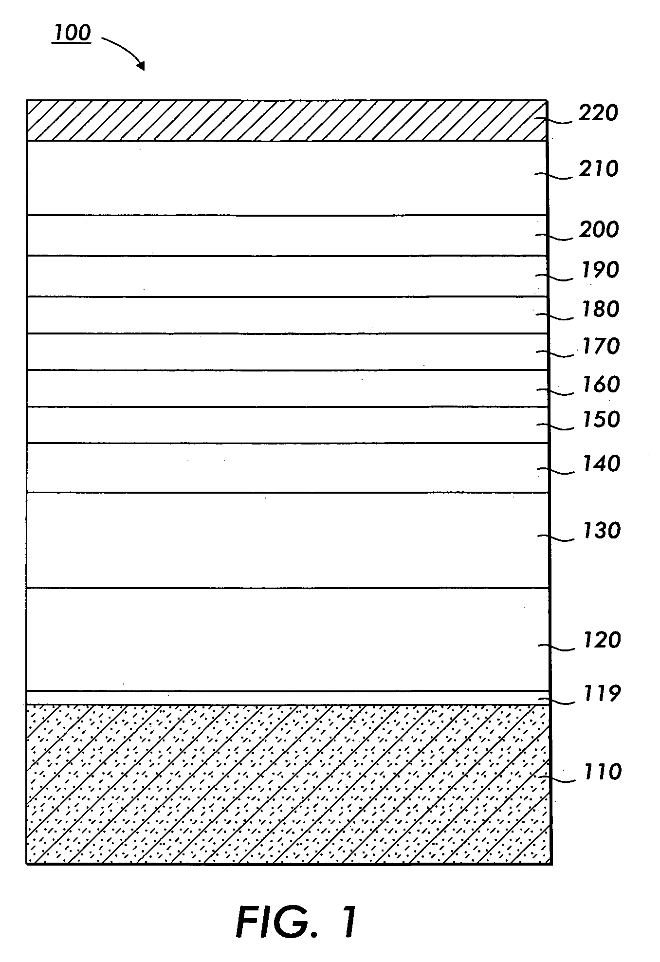
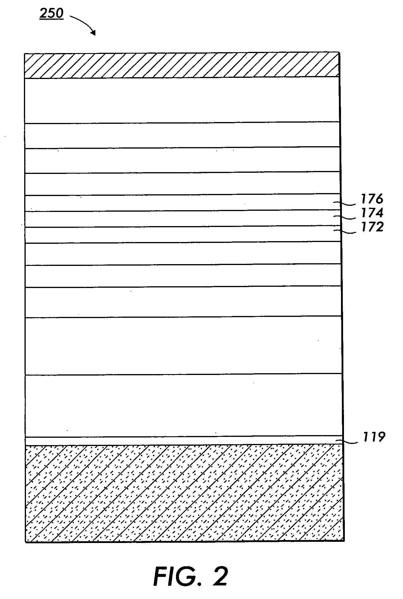
[0037] The short diffusion length of carriers in gallium nitride heterostructures requires that the carrier donor sites be located very near the quantum well active region, so that the carriers reach the active region before recombining. However, magnesium doping of a GaN heterostructure, which provides the positively-charged carriers (i.e., holes), has a very high ionization energy. For example, the ionization energy for Mg acceptor atoms in GaN is about 200 meV. As a result, for an Mg acceptor concentration of about 1020 atoms per cm3, only 1018 holes per cm3 are obtained. Furthermore, the Mg ionization energy in AlGaN compounds increases with increasing Al content at a rate of about 3 meV per percent mole fraction of aluminum, requiring even more donor atoms per generated carrier. Because only 1% of the donor atoms are ionized to produce a charge carrier, very high doping levels must be implemented in GaN or AlGaN films to generate sufficient carrier densities to produce gain.

[0...


PUM


Abstract

A pair of undoped spacer layers are provided adjacent to, or near to, a single quantum well aluminum gallium nitride active region. In various exemplary embodiments, the undoped spacer layers are provided between the single quantum well aluminum gallium nitride active region and carrier confinement layers. The undoped spacer layers reduce the threshold current for the laser device and improve the output characteristics.

Description

REFERENCE TO GOVERNMENT CONTRACT [0001] This invention was made with Government support by the DARPA SUVOS Program under SPAWAR Systems Center Contract No. N66001-02-C-8017, and the Government has certain rights in this invention.BACKGROUND OF THE INVENTION [0002] 1. Field of Invention [0003] This invention is directed to semiconductor laser diodes emitting in the ultraviolet region of the spectrum. [0004] 2. Description of Related Art [0005] In recent years, gallium nitride-based compound semiconductors, such as GaN, InGaN, GaAlN, and InGaAlN, have received a great deal of attention as materials for violet- and blue-emitting semiconductor lasers. Semiconductor lasers using these materials in the multi-quantum well (MQW) active region are designed as short-wavelength laser sources. Hence, their output can be focused to small diameters. Owing to this advantage, these lasers are expected to be usable as light sources for high density information storage, such as in an optical disk. [0...

Claims


Application Information

Patent Timeline
Patent Type & Authority Applications(United States)
IPC IPC(8): H01S5/20H01S5/34H01S5/343
CPCB82Y20/00H01S5/2009H01S5/3407H01S5/3408H01S5/34333
Inventor KNEISSL, MICHAEL A.TREAT, DAVID W.
Owner PALO ALTO RES CENT INC
Why Eureka
Try Eureka