Semiconductor memory device and manufacturing method for the same
- Summary
- Abstract
- Description
- Claims
- Application Information
AI Technical Summary
Benefits of technology
Problems solved by technology
Method used
Image

Examples
embodiment 1
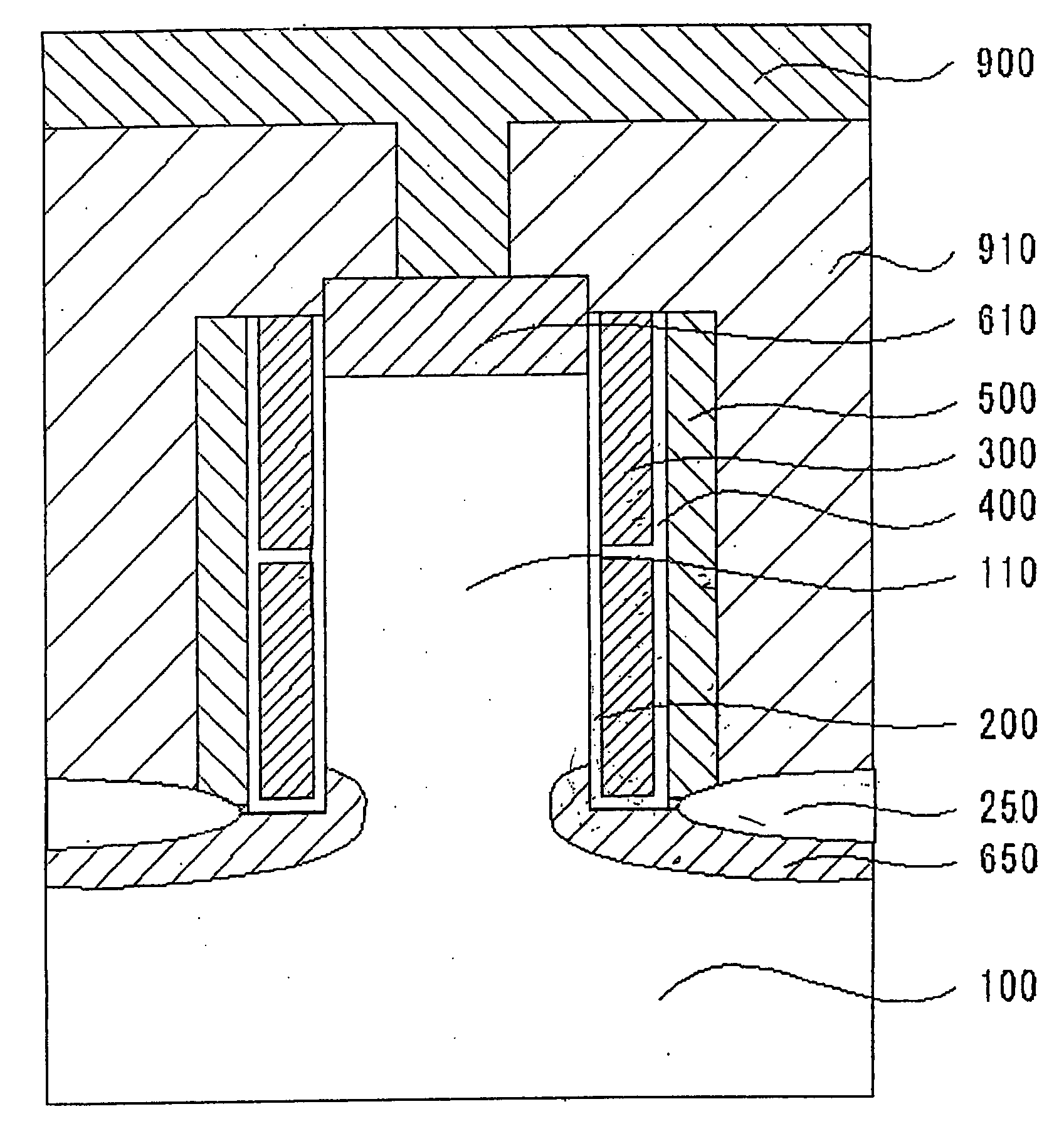
[0055]FIG. 1 is a schematic cross section of a memory cell according to Embodiment 1. In the figure, reference numeral 100 denotes a p-type semiconductor substrate, 110 a columnar semiconductor portion, 200 a tunnel oxide film, 250 a device isolation film, 300 charge-storage layers (floating gates), 400 an interlayer insulating film, 500 a control gate, 610 and 650 source / drain diffusion layers, 900 a metal wiring, and 910 another interlayer insulating film.
[0056] In Embodiment 1, at least one p-type columnar semiconductor portion 110 is formed on the p-type semiconductor substrate 100 made of silicon. At least a portion of a periphery of the columnar semiconductor portion 110 serves as an active region surface. The tunnel oxide film 200 is formed on at least a portion of the active region surface. Also, the charge-storage layers 300 made of, for example, polycrystalline silicon that are divided in a direction vertical to the p-type semiconductor substrate 100 are formed to cover a...
embodiment 2
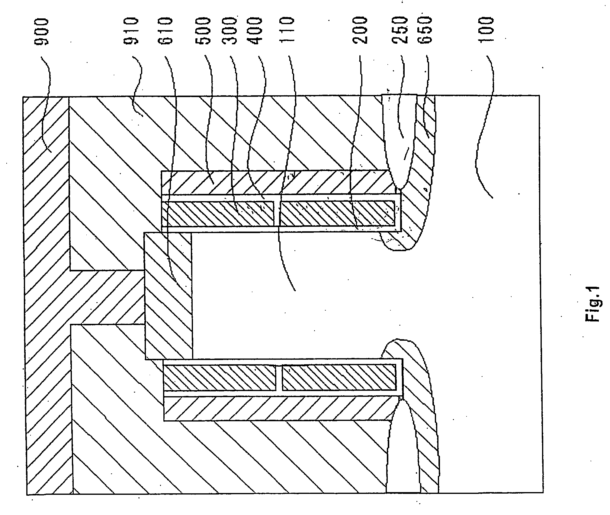
[0057] A memory cell shown in FIG. 2 has the same construction as that in Embodiment 1 except that a control gate 510 is made of a metal. Examples of the materials of the control gate 510 include metals such as aluminum, tungsten, copper and the like. Since the control gate is made of a metal, it is possible to reduce the resistance of wordlines and suppress the wiring delay and the like.
embodiment 3
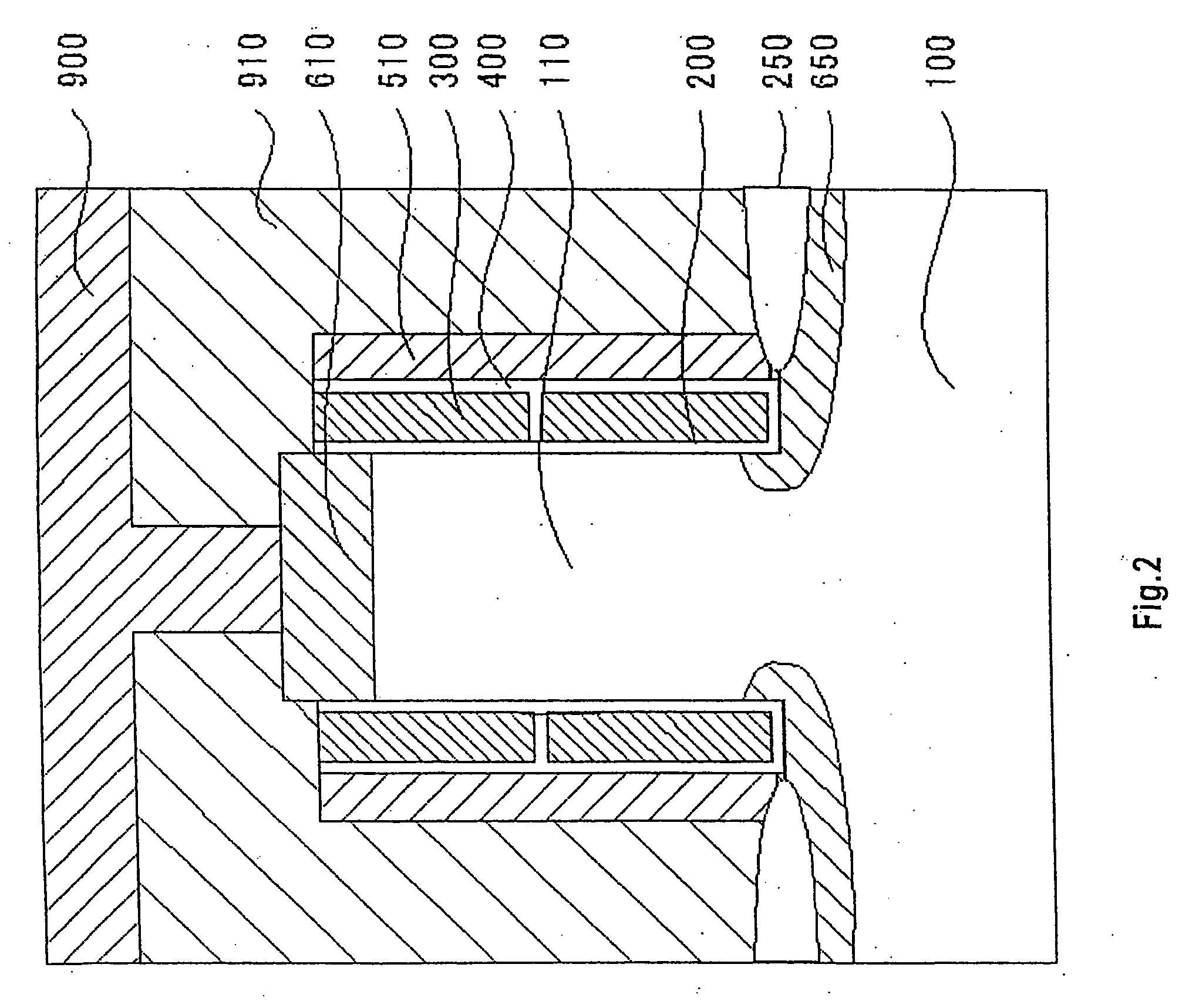
[0058] A memory cell shown in FIG. 3 has the same construction as that in Embodiment 1 except that the columnar semiconductor portion 110 is made of n-type silicon. In this embodiment, the source / drain diffusion regions 610 and 650 that are formed respectively above and below the columnar semiconductor portion 110 are of a p-type, the conductivity type opposite to that of the columnar semiconductor portion.
Theories of Operations of the Memory Cells According to Embodiments 1-3
[0059] The above semiconductor memory devices have a memory function provided based on the conditions of a charge stored in the charge-storage layers. In the below, the theories of a read out operation, a write operation and an erasure operation will be described by taking the memory cell shown in FIG. 1 as an example.
(1) The Theory of the Read Out Operation will be Described Below.
[0060]FIG. 4 shows an equivalent circuit of the memory cell of FIG. 1, and FIG. 5 shows an example of a timing chart at the re...
PUM
 Abstract
Description
Claims
Application Information