Process for fabrication of printed circuit boards
a printed circuit board and fabrication technology, applied in the field of process and apparatus, can solve the problems of poor chemical stability, low conductivity, unsuitability for many electronic circuits, etc., and achieve the effect of less cos
- Summary
- Abstract
- Description
- Claims
- Application Information
AI Technical Summary
Benefits of technology
Problems solved by technology
Method used
Image

Examples
first embodiment
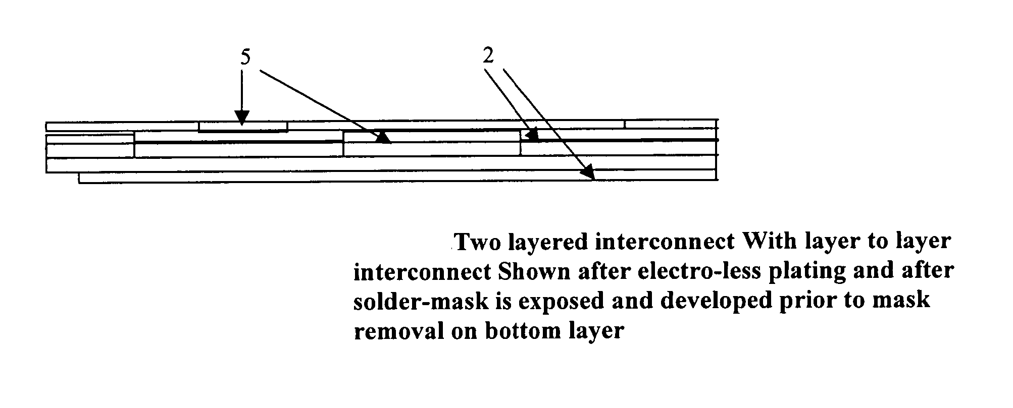
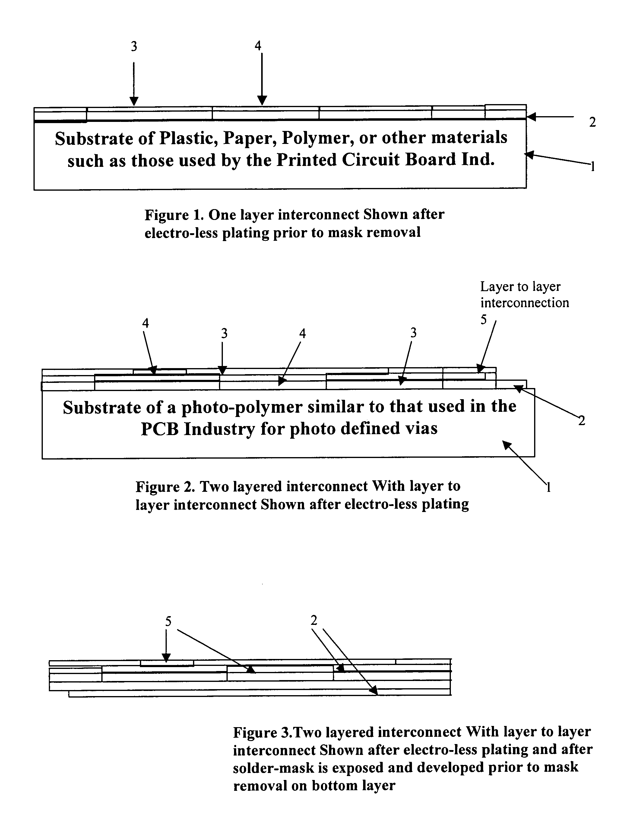
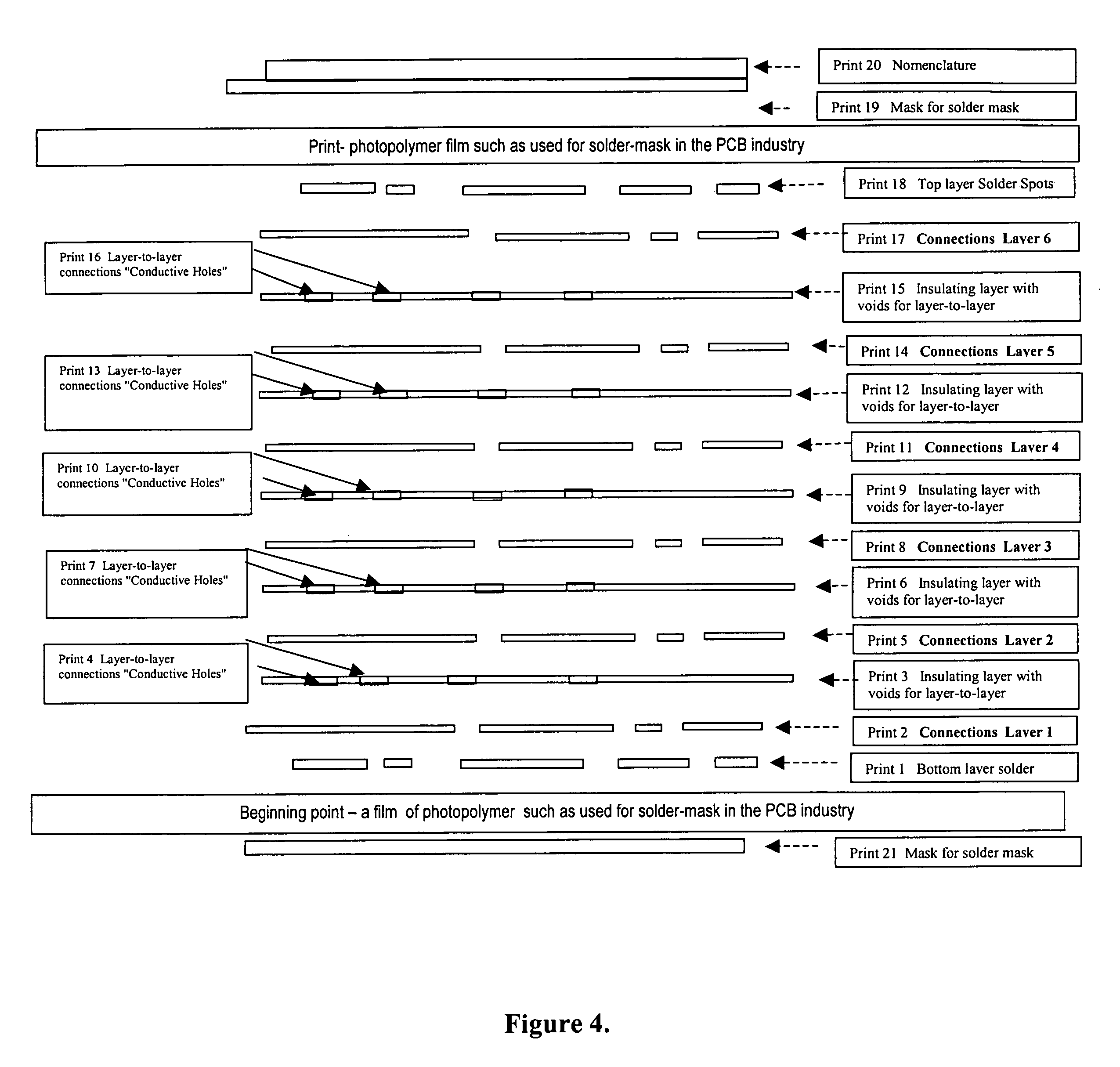
[0022] As shown in FIG. 1, the fabrication process begins with the application, upon a substrate 1 such as paper, plastic etc., of a thin film of a suitable low conductivity polymer coating solution such as Baytron which is a commercially available low conductivity polymer which is available from Bayer Material Service, A.G., and is sold as an aqueous solution of poly (3, 4-ethylenedioxythiophene)-poly (styrenesulfonate) or “PEDT / PSS”, or any other suitable polymer, which is then laced with small quantities of a catalytic reducing agent. The preferred reducing agent is an aqueous dispersion of nano-particle palladium. Whatever reducing agent is used it should be compatible with the polymer coating. The combination of a suitable polymer with a compatible reducing agent dispersion 2 is coated or printed on to receptor substrate 1. The coating 2 allows for the forming of complex circuit patterns. To facilitate coating, wetting agents and suitable cross-linking agents and materials such...
second embodiment
[0026] this fabrication process involves formulating and applying an ink-jet composition directly to the receiving surface to create the coating layer 2, which is then electro-less plated, as previously described. This creates the circuit image directly, but is limited by the resolution and image quality of ink jet printing process.
[0027] In this second embodiment, the first step is coating the entire substrate with a polymer and the reducing agent. Next, a mask is printed lithographically or otherwise masked with a normal printing method. Finally, the masked substrate is electrolessly plated. Preferably the substrate is first plated with nickel, then with copper. Finally a second layer of nickel is applied, which creates a hard surface.
[0028] This process leaves printing ink in the circuit, which is normally a good thing. Ink is hard to remove and is very stable. Furthermore, by using a solvent based ink which contains both the polymer and the reducing agent, the ink can be used t...
third embodiment
[0029] A third embodiment involves using electro-photography and lithographic or offset printing to create the coating layer 2, which is then electro-less plated as previously described. This results in much higher resolution images and if pre-coated webs are made for the lithographic process, low cost, high speed, high volume repeat circuits can easily be manufactured. The use of electro-photography allows each image to be different and is ideal for prototype circuits where the desired quantity is low. Different masking patterns could be printed and used as required.
[0030] Subsequent steps in circuit manufacturing, such as application of a solder mask and protective coating can be accomplished by techniques well known in the art. The imaging of the photopolymer would be simplified by printing the mask, by electro-photographic printing or lithographic printing, directly on the photo polymer and thereby achieving higher resolutions than can be obtained on masks by screen-printing.
[0...
PUM
| Property | Measurement | Unit |
|---|---|---|
| Electrical conductor | aaaaa | aaaaa |
| Wetting tension | aaaaa | aaaaa |
Abstract
Description
Claims
Application Information
 - R&D
- Intellectual Property
- Life Sciences
- Materials
- Tech Scout
- Unparalleled Data Quality
- Higher Quality Content
- 60% Fewer Hallucinations
Browse by: Latest US Patents, China's latest patents, Technical Efficacy Thesaurus, Application Domain, Technology Topic, Popular Technical Reports.
© 2025 PatSnap. All rights reserved.Legal|Privacy policy|Modern Slavery Act Transparency Statement|Sitemap|About US| Contact US: help@patsnap.com